Issued Date: 2019/3/14
Issued By: iST
As processes shrink ever smaller, how can we perform FIB circuit editing successfully?
As predicted by Moore’s Law, the IC process is continuously shrinking from 1um, 0.5 um, 0.13um, down to the nm scale, which must be challenges to FIB labs’ tech development and application capabilities. Especially for processes below 16nm, as most of ICs package types are flip chip packages and backside circuit editing is only one method. Thus, the difficulty is greater and greater.
Since 2018, iST’s FIB circuit edit lab has received many samples from 7 nm process nodes requesting backside circuit editing. It was said that the task is such a tall order that iST’s competitors found no way to deal with it. iST has been specializing in IC FIB circuit editing since its foundation. It executed front-side circuit editing for 20/16 nm ICs in 2015, backside FIB circuit editing for 16nm ones in 2016 (refer to figure 1), and has done the same for 7nm ones successfully recently.
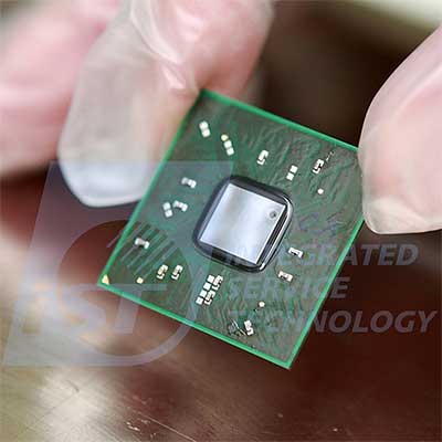
Figure 1: Example of backside FIB circuit editing.
iST Tech Classroom will now present the challenges in backside circuit editing for advanced processing and 7nm ICs, and the steps taken by iST in dealing with this tall order.
I. The more shrunk the 7nm circuit, the more difficult the circuit edit
The fundamental requirement of any process is to have IC samples after FIB circuit editing ready for electrical testing. Before that, iST engineers will review the following three key-points with this in mind:
- Learn about the characteristics and the editing purpose of the IC circuit designed by you;
- Propose circuit layout and review areas that can be damaged;
- Pinpoint the best target point and broach the feasibility of circuit editing.
The density of transistors on wafers is up by many times as the design rules shrink; the 7 nm process technology from this year would raise density by 350% in each square millimeter over its 16 nm counterpart, let alone other greater difficulties. No matter what, all these three are critical to FIB circuit editing and deserve your closest attention
II. The two key factors of backside circuit editing – the thickness remaining of the pre-treatment substrate and location of the end point
Firstly, the package type will determine the thickness of silicon substrate. Most of the wafers would be thinned down to 8~12 mil from 31 mil, which is too thick to edit any micron/nano grade FIB circuit directly. According to the first step of the aforementioned 3-step process, we start to define the partial milling area of the silicon layer (milling silicon trench, maximum size 350*350um); two key points here are to improve flatness in the trench’s inner surface (refer to figure 2) and determine the location of the end point (refer to figure 3) to prevent over-etching (refer to figure 4); taking 7 nm as an example, it’s better to leave silicon thickness at 1~2 um (refer to figure 5) as this is the key factor before circuit editing.
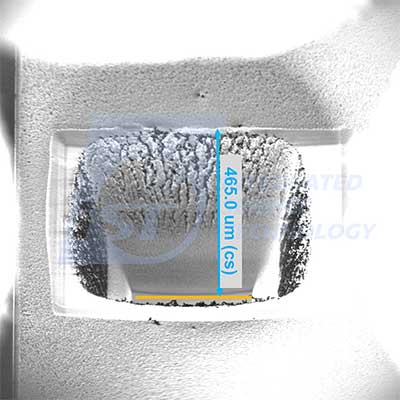
Figure 2: The depth of the silicon layer is 465um thick; surface of trench bottom remains flat after milling by iST (yellow line) to maintain etching precision by milling head.
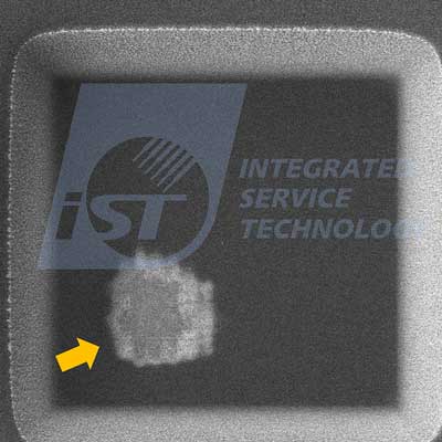
Figure 3: Components in active area exposed (indicated by the arrow) due to trench milling resulting in a non-flat surface or missing the end point.
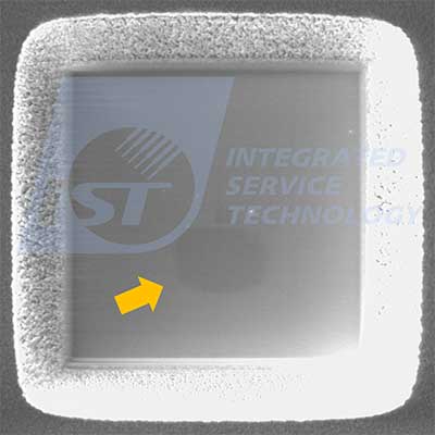
Figure 4: Determine milling end point accurately (indicated by the arrow).
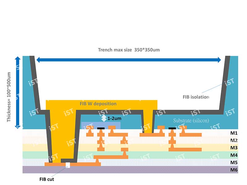
Figure 5: Backside circuit edit illustration; it’s better to keep the silicon layer 1~2 um thick.
III. Accurate target positioning and clear circuit identification
The width, thickness and gap between dielectric layers and metals of advanced processes, especially the 7 nm one, almost goes down to 40 nm or less. The largest challenge of facing thinner and smaller process technology is to position targets accurately and identify circuits clearly. Further, the circuit editing operation is a process measured in units of “seconds,” which tends to spoil all your efforts in one fell swoop.
How to position targets with high precision?
Since it is impossible to view circuits through electron microscope imaging during backside editing, you are required to position the circuit by its four corners with an infrared camera first to align GDS and the chip, and follow this by multiple positioning on one or more reference points to get close to the target by 100 um or less (the farther away, the more severe the error). It’s recommended to be no more than 20 um away from the target point. Additionally, about a 2*2 um area can be destroyed as the positioning point to reduce actual error down to 150 nm.IV. Calibrate etching parameters and gas to prevent metal layer over-exposure
Poor parameter and gas selection in editing circuits of advanced processes may lead to either over-etching and unrecoverable open circuits or exposure of non-essential metal layers. Both may be overlooked in advance processing. For example, if the point requires connection to another position, the deposited metal line would result in circuit short and leakage between the metal layers. This would leave IC samples with failure or unexpected electrical characteristics (refer to figure 6, 7, and 8). It is necessary to tune up the best etching parameters and gas to prevent metal layer over-exposure.
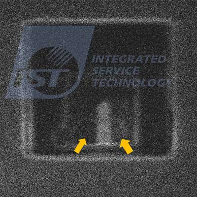
Figure 6: Etching results in boring (indicated by arrows) exposed the underlying metal layer; deposited metal conductor results in shorting and leakage between the metal layers.
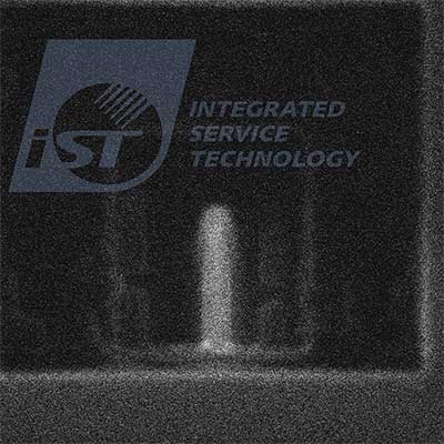
Figure 7: Compare against the same position in figure 6: a flat etched surface without metal layer exposure in the non-target range.
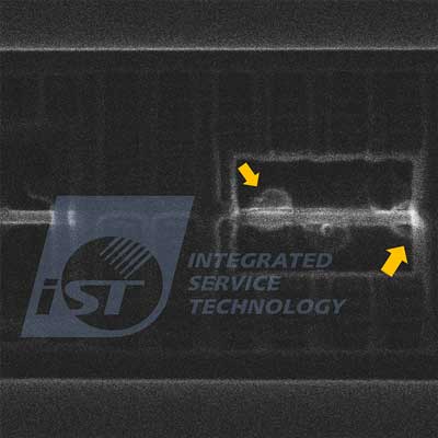
Figure 8: Uneven etched surface (indicated by arrows) and found the metal layer exposure in non-target range.
This article is aimed to share our experiences with honorable clients like you. In case you want to know more details, please call Mr. Chino Wang at +886-3-579-9909 Ext. 6000 or email: web_fib@istgroup.com