Issued Date:2024/1/02
Issued By:iST
FIB-SEM (Focused Ion Beam-Scanning Electron Microscopy) has applications in materials analysis, electronics, and nanotechnology. It enables accurate sample preparation, high-resolution imaging, and 3D reconstructions. Importantly, it analyzes microscopic flaws, prepares TEM samples, and studies nanoscale complex structures. This article explores the capabilities, applications, and benefits of FIB-SEM.
What is FIB-SEM?
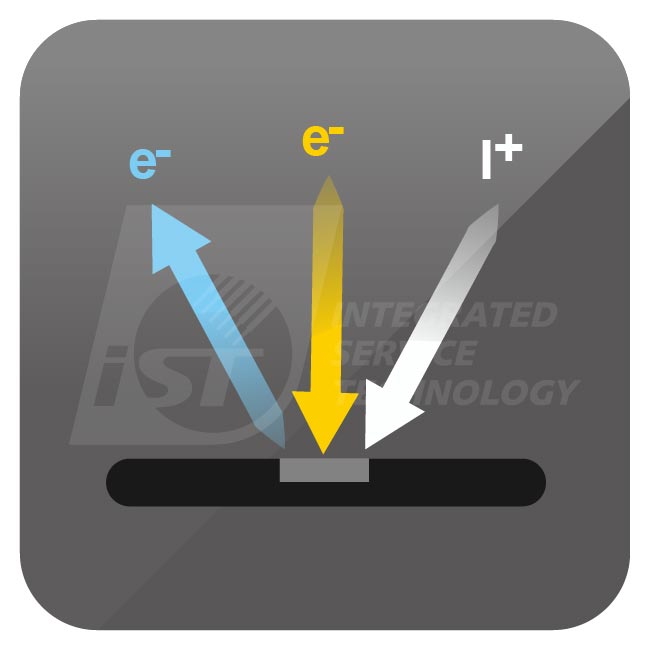
FIB-SEM combines the nanometer-scale precision of a Ga+ focused ion beam with the high-resolution imaging of a scanning electron microscope for 3D tomography, site-specific sample preparation, and material analysis. The FIB utilizes a gallium ion source to mill and sputter samples from 500V to 30kV. It enables precision cross-sectioning and thinning of samples; sub-nanometer structural and compositional details are key. To examine delicate, beam-sensitive materials, the SEM(Scanning Electron Microscope)can image milled surfaces with typically 3~5 nm resolution at low accelerating voltages around 1kV.
This system assures consistent spot size, precise navigation, and low-energy operation to minimize FIB-induced damage. It is widely used in semiconductor failure analysis and nanoscale structure analysis, preparation ultrathin TEM lamellae, defect resolution, and atom probe tomography. Its ability to control and observe nanoscale materials makes it essential for applications requiring atomic-level insights and 3D structural accuracy.
Key Capabilities and Advanced Functionalities of FIB-SEM (Dual Beam FIB)
High-Resolution Imaging
FIB-SEM delivers nanoscale, high-resolution imaging for material characterization, particularly in semiconductor analysis with fine device features. Low-voltage imaging maintains resolution for beam-sensitive materials, while gallium ion channeling enhances contrast to reveal subtle grain structures. Automated SEMcalibration ensures repeatable, accurate performance.
Precise Material Removal
The FIB enables nanometer-precision material removal, ideal for cross-sectional analysis and TEM sample preparation, requiring ultrathin sections (<50 nm). Beam energy and current can be adjusted for either rapid milling or low-damage thinning to isolate defects without compromising surrounding structures.
3D Reconstruction
While single-beam FIB can perform sequential sectioning, it cannot image the same section it mills. In contrast, Dual Beam FIB-SEM excels by allowing immediate imaging of each milled section, enabling precise and detailed 3D reconstruction of the sample with ease.
Elemental Analysis
Integrated with energy-dispersive X-ray spectroscopy (EDS), FIB-SEM maps elemental distributions with spatial resolutions detecting trace elements. Combined with WDS and TOF-SIMS, it enables advanced chemical and isotopic analyses for research and industry applications.
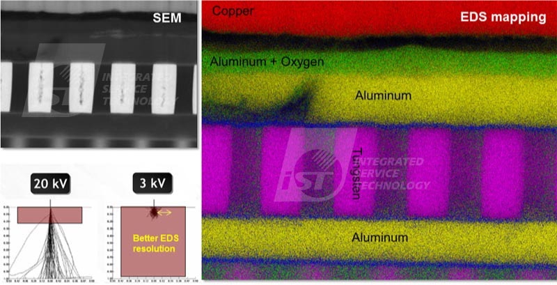
The large window (up to 150mm2) EDS detector comes with excellent spatial resolution for advanced application of “concurrent cutting, shooting, and analyzing”.
Applications of FIB-SEM

- Semiconductor Industry: FIB-SEM enables precise cross-sectioning and high-resolution imaging to investigate nanoscale defects, voids, and dislocations in ICs. It helps diagnose failures, improve yield, and validate device reliability in advanced semiconductor nodes.
- Materials Analysis: Microstructure analysis of metals, ceramics, and polymers can reveal critical details such as grain boundaries, phase distributions, voids, and inclusions, particularly in semiconductor materials. Using FIB-SEM, these insights help evaluate alloy strength, detect defects in ceramic layers, and analyze polymer matrix compositions, supporting failure analysis and improving material performance in semiconductor applications.
- Nanotechnology: Nanostructures like nanowires and nanoparticles can be fabricated and characterized using FIB-SEM. With its ability to perform ultrathin cross-sectioning and 3D reconstruction, it provides insights into growth mechanisms and structural fidelity, ensuring reliable performance in nanoelectronics and photonics applications.
Sample Preparation for FIB-SEM
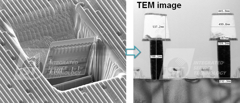
Prepare TEM sample up to 15nm thin.
Importance of Sample Preparation
Sample preparation is essential for achieving accurate results in FIB-SEM analysis. The quality of initial preparation directly impacts image resolution, clarity, and the accuracy of elemental mapping or 3D reconstruction.
For instance, in semiconductor failure analysis, improperly prepared samples may hide faults or introduce artifacts that skew results. At the same time, poor preparation in materials science may generate uneven surfaces that hinder cross-sectional imaging or material redeposition during milling, which may obscure critical features.
Challenges in Sample Preparation
Ion implantation or surface amorphization during FIB-SEM sample preparation can alter material properties, making it crucial to preserve structural fidelity and ensure electron transparency for TEM analysis. The heterogeneity of a sample—such as variations in density or composition—further complicates preparation, adding to the complexity of achieving accurate results.
Techniques for Effective Preparation
Accurate FIB-SEM analysis relies on proper sample preparation. Protective capping layers prevent ion beam damage and material redeposition, while low-energy ion milling minimizes damage for delicate samples. Gas-assisted etching improves milling efficiency and surface quality for materials like silicon dioxide. Final thinning at low energy and currents ensures electron-transparent lamellae for high-resolution TEM analysis.
The Dual Beam FIB-SEM system combines precise ion milling and high-resolution SEM imaging, streamlining 3D reconstruction and in-situ TEM sample preparation for efficient, accurate analysis.
iST Material Analysis Laboratory has been working in the semiconductor and advanced packaging fields for a long time and has accumulated considerable experience and successful cases. If you have any related needs or want to further understand the relevant knowledge, please feel free to contact Dr. Weijui Lin at +886-3-579-9909 ext. 6166 or email at web_ma@istgroup.com;marketing_tw@istgroup.com。