Issued Date:2024/06/26
Issued By:iST
The 21st century is the semiconductor century, especially Si-based semiconductors. The manufacturing technique of mass production of Si-based semiconductors has progressed from several ten-um nodes to the 3 nm node within less than 40 years. The configuration of high-end semiconductor devices is very complicated, the thickness of thin films in the key structure has approached sub-nano meter. Microscopes with sufficient resolving power have to be used to check the dimension routinely.
Traces of dislocations
The resolution of several kinds of microscopes is shown in Figure 1. TEM/STEMs are the only microscope family with resolving power of atomic level. The more accurate control in the configuration of semiconductor devices during processes, the higher the yield will be, and so is the benefit. That’s why many TEM/STEMs are currently used in semiconductor manufacturers.
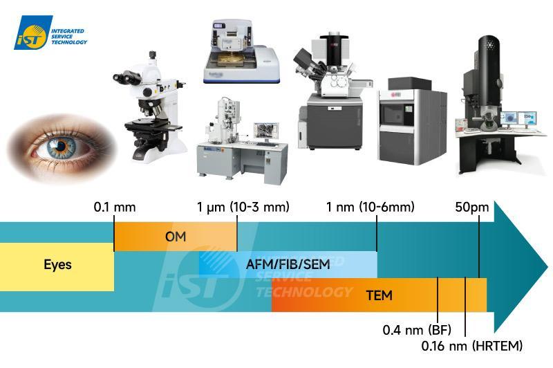
Figure 1. Resolution of microscope family.
(Source: iST)
1. Why Perform TEM
Besides atomic-scale resolution in images, the spatial resolution of TEM/STEMs reaches the sub-nanometer. Chemical information as well as structural information and crystallographic information of semiconductor devices can be characterized by TEM/STEMs. A typical example is shown in Figure 2. The HRTEM image can reveal the dimensions of thin films down to sub-nano-meter accurately but is not able to tell what these thin films are. With the aid of STEM/EDS maps, thin films of Hf-oxide, aluminum, titanium, …on the fin can be revealed. By TEM/STEM characterization, works of R&D and yield improvement in semiconductor manufacture can be more effective and efficient.(read more: New TEM Auto Metrology Helps Overcome 2nm Manufacturing Bottleneck)
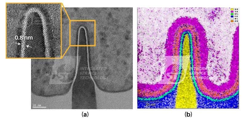
Figure 2. TEM/STEM data of a FinFET structure. (a) HRTEM image, (b)EDS elemental map.
(Source: iST)2. How is TEM Performed
Since the configuration of semiconductor devices is meticulous and complicated, the size of the devices of high-end IC is usually very large. All TEM specimens of semiconductors thus have to be taken from precisely specified positions in chips to extract interesting and useful data. Currently, more than 99% of TEM specimens of semiconductor devices are prepared by FIBs that can make TEM specimens from exactly specified positions. The analyzable area of TEM samples is usually limited to less than 15 um x 8 um to avoid specimen bending. Specimens for high-quality HRTEM and HRSTEM analysis are usually thinner than 50 nm in thickness, the available area is then usually restrained to be smaller than 8 um x 4 um to keep the specimen as flat as possible.
Typically, TEM/STEMs used to analyze semiconductor devices are operated at 200 KV. Electrons of high coherency are emitted from a field-effect electron gun (FEG), accelerated to 200 KeV, then manipulated by condenser lenses and objective lenses to penetrate the specimen in a focused or non-focused electron beam. These high-energy electrons have characteristics of both the particle and wave simultaneously. A set of electron diffraction patterns is formed first at the back focal plane of the objective lenses when high energy electrons pass through the thin foil specimen, the first image is formed at the first image plane a little distance forward.
Interaction between incident electrons and the specimen occurs when high-energy electrons pass through the thin foil specimen. Interactions can be divided into elastic scattering and inelastic scattering from the point of energy. Electron diffraction patterns and TEM/STEM images are formed mainly by elastically scattered electrons. Chemical data of the specimen are analyzed by EELS and EDS, using inelastically scattered electrons and X-ray signals generated from the specimen after being knocked by incident electrons respectively.
Today, the progress of precision machining and computer control has merged them into a TEM/STEM system that can perform all analyses mentioned, as shown in Figure 3, and all data (images, patterns, spectra) are stored digitally. Several new techniques have been developed by auxiliary of a high-performance computer which replaces a microprocessor in TEM operation.
3. When to Perform TEM
During the last decade, the demand for increasingly higher-performance semiconductor products has stimulated the semiconductor industry to respond by producing devices with increasingly complex circuitry, more transistors in less space, more layers of metal, dielectric, and interconnects, in less space. Following the progress in semiconductor manufacturing processes, demand for microscopes with higher resolution for more accurate measurement and characterization dramatically increases. The atomic scale imaging resolution and nanometer scale composition analysis and diffraction resolution provided by modem TEM/STEM systems are particularly well suited for solving materials problems encountered in the process development, manufacture controlling, and failure analysis. TEM has very high resolution but poor sampling abilities. Each TEM specimen contains an area of less than 120 um2 (1.2 x 10⁻⁴ mm2). So, it wastes time and resources to characterize the whole device by TEM. TEM is used to characterize those key structures only. Before using TEMs to look at the veins on leaves, visible light microscopes and scanning electron microscopes (SEMs) should be used first to check the forest and trees.
Application of TEM in the Semiconductor Manufacturing Process
TEM-based techniques are suited for evaluating interfacial details, dimensions of nanodevice structures, and defects or flaws that arise during the fabrication process. Typical key structures analyzed by TEM include gate oxide (SiO2 or SiON) in MOS structure and FinFET structure, as well as high-k metal gate and silicide. The dimension of GOX is around 1.0 nm, thus accurate measurement of gate oxide thickness is necessary because even a 0.1 nm decrease in oxide thickness can lead to an order of magnitude increase in leakage current.
When some new functional materials are introduced into novel semiconductor devices by nano thin film morphology, characterization of these materials by high image resolution and high spatial resolution in chemical analysis, leading to a full understanding of their working principles, is absolutely necessary.(read more: How to Identify & Analyze Ga2O3?)
During the progress in semiconductor manufacturing processes and scaling down the feature sizes, transmission electron microscopy (TEM) has played a very important role in the process development, manufacture controlling, and failure analysis by its atomic scale imaging resolution nanometer scale composition analysis, and diffraction resolution.
The only shortage of TEM analyses is the limited sampling size. Many specified site specimens are then needed to fully characterize feature structures in novel semiconductor devices. Numerous TEM samples inevitably have to be made within a short period to meet the fast rhythm of R&D in the semiconductor industry. Almost all TEM specimens of semiconductor devices are prepared by the FIB. The characteristics of accuracy, high yield, and short turn-around time of FIB make this TEM sample preparation technique highly attractive in the semiconductor industry.