Issued Date:2025/7/22 3D Surface
Issued By:iST
Using inappropriate metrology may lead to a drop-in product yield, misjudgment of processes, delayed schedules, and even a complete batch scrap. As advanced processes like AI chips, CoWoS, and HPC rapidly progress, every critical step relies on high-precision surface topography measurement. The problem is, the suitable analysis methods vary significantly for different samples. Are you really choosing the right one?
3D Surface
Alongside the growth of AI chips, high-performance computing (HPC), and advanced packaging technologies such as CoWoS, the demands on process control and metrology precision are intensifying. From wafer manufacturing, etching, and deposition to die packaging and module assembly, surface metrology helps ensure quality control and process stability.
What is “surface topography measurement”? Simply put, it’s measuring the microscopic ups and downs, roughness, curvature, flatness, and other geometric characteristics of a sample’s surface. This data helps in understanding whether a material or process is stable, if there are any abnormalities, and consequently impacts subsequent yield and product reliability.
Using inappropriate analysis methods may lead to misjudging defect origins, repeated testing, delayed schedules, increased costs, reduced yields, and lower product reliability. At iST, we’ve observed that “selecting the wrong analysis” is a common pitfall for engineers.
Depending on the product application, this iST Tech Classroom will introduce four major advanced surface metrology and their optimal usage scenarios to help engineers work smarter.
3D Surface
3D Surface
In the semiconductor industry, optical microscopes (OM) and contact profilometers have long been indispensable tools for surface inspection and basic measurements. However, as structures become increasingly intricate in advanced applications like AI chips, High-Performance Computing (HPC), and CoWoS, these traditional methods face growing challenges. They often lack the resolution needed to capture nanoscale details, their contact probes can potentially damage delicate samples, and their measurement efficiency and accuracy fall short of the demands of rapid development cycles.
It’s precisely in these areas—where high-precision, non-contact, and high-efficiency measurements are critical—that several advanced surface topography measurement technologies have emerged. These innovations provide crucial support in overcoming process bottlenecks, and we’ll introduce them to you one by one below.
1. Surface 3D Profiler: Ideal for Packaging, Modules, PCBs, and High-Step Products
Designed to solve the limitations of traditional measurement tools, the Surface 3D Profiler offers non-contact, high-speed 3D scanning over large areas. It uses optical fringe projection to cast light patterns on a sample; surface height variations distort the pattern, which is then converted into height data based on known incident angles.
Easy to use, this tool automatically scans the area, height, and curvature of a sample without the need for complex pre-processing. With built-in auto-alignment and high-resolution algorithms, it improves data stability and repeatability, minimizing human interference.
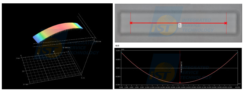
Figure 1: Compared to traditional methods, the Surface 3D Profiler allows for one-click surface topography measurement.
(Source: iST)The Surface 3D Profiler that iST has implemented is equipped with Fringe Projection and HDR (High Dynamic Range) scanning technology. This allows us to accurately acquire data from challenging samples, including highly reflective materials (like CoWoS and wafers), low-reflectivity materials (like black molding compounds), and even transparent samples, thanks to its built-in compensation features.
With a maximum measurement range of 300×150×70 mm and up to 25 million data points, this profiler can cover everything from small dies to large modules. It boasts impressive repeatability, achieving 0.4 μm in height and ±5 μm in width.
This Profiler is widely applied across a variety of samples, including wafers, bare dies, packages, BGA, capacitors, IC chips, passive components, CSP, PCB, PCBA, QFN, connectors, and sockets. This makes it an ideal solution for comprehensive quality control and process monitoring, from pilot runs to full-scale production lines.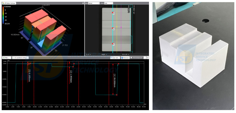
Figure 2: The Surface 3D Profiler deployed by iST can acquire all necessary step heights and surface dimensions from a single scan of a step gauge (right image).
(Source: iST)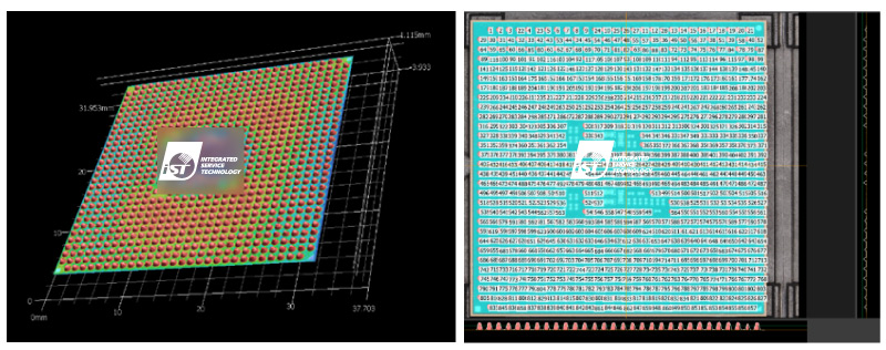
Figure 3: The Surface 3D Profiler utilized by iST can automatically extract BGA solder ball regions, calculate the height of each ball, and determine overall coplanarity, effectively helping to confirm the warpage profile of the component’s solder ball area.
(Source: iST)2. White Light Interferometer (WLI): Suitable for Large-Sized, Non-Transparent Material Samples
WLI employs the theory of optical interference (Figure 4), i.e., spacing of constructive interference fringes equal to the fixed wave path difference, to calculate the height into a 3D topography based on surface profiling (Figure 5) which, in turn, is used to calculate surface roughness and provides nanometer-level height resolution through non-contact measurement. WLI is ideal for samples of a larger size, up to 100um or even a couple of millimeters, as it relies on optical microscope for the measuring.
WLI is most likely adopted for profiling the surface of opaque materials including metals, circuits, plastics rather than translucent ones (e.g., glass). Other analysis technology is required when the surface of the material under test cannot be applying metal plating for WLI measurement.
For example, post-acid-washed metal surfaces (300 μm² area) measured with WLI show average roughness (Ra) greater than 1 μm.
See Figure 6 for a metal surface after acid cleaning and its roughness (average greater than 1um) measured over a surface square of 300um.
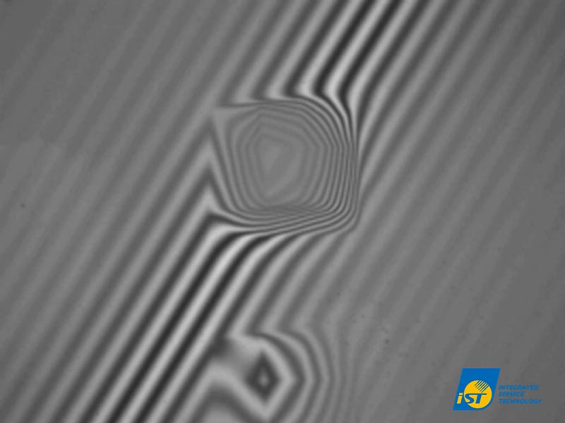
Figure 4: White light interference
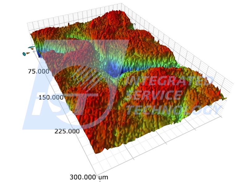
Figure 5: 3D profiling
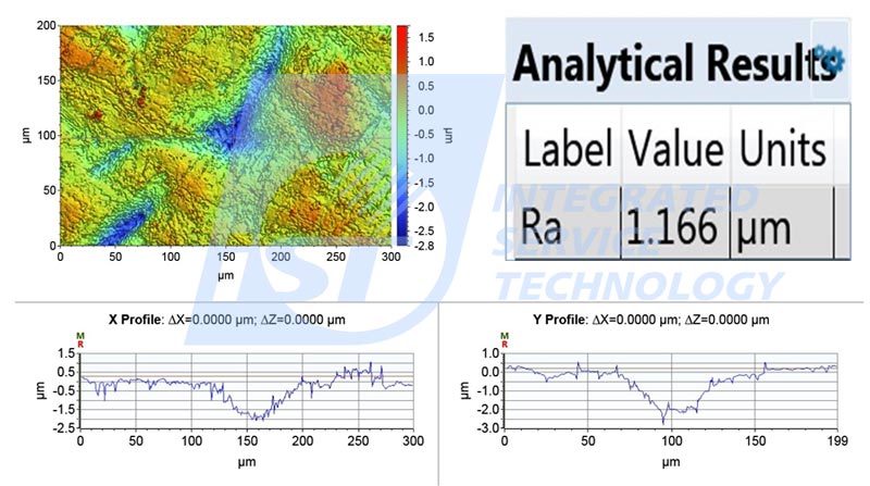
Figure 6: 2D/1D profiling and roughness analysis in the value of Ra
(Source of figure 4~6: iST)3. Atomic Force Microscope (AFM): Suitable for Wafer and Glass Material Samples
AFM employs nanometer-radius silicon probe to profile samples of very flat surfaces or soft polymers (e.g., photoresist) for surface roughness measurement. It is widely adopted in micro analysis over an area of tens of microns on the surface of the wafer or glass pre- and post-cleaning, coating and etching.
In recent years, AFM has been increasingly used for surface measurement and monitoring in research related to Integrated Circuit (IC) processes such as Chemical Mechanical Polishing (CMP), Redistribution Layer (RDL), and Under Bump Metallization (UBM), both before and after their etching stages. This is crucial because abnormal roughness can lead to subsequent thin film delamination or even reliability issues.
As shown in Figure 7, the profile of a 2um square surface on PI polymers with an average roughness at around 8nm. To accurately compare its pre- and post-roughness, a non-destructive measurement method is essential. While AFM (Atomic Force Microscopy) provides the necessary measurement capabilities for such nanoscale features, the device must also be able to accommodate samples larger than 300mm, specifically for measuring 12-inch wafers.
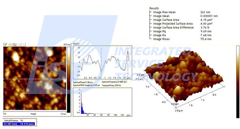
Figure 7: AFM profiling and roughness analysis in value of SAD%, Rq and Ra (Source: iST)
4. Shadow Moiré: Ideal for Thermal Warpage Analysis of Package Substrates or PCBs
Shadow Moiré involves creating interference fringes between a grating and the sample surface to measure warpage. It’s particularly useful for analyzing thermal deformation in substrates and PCBs. In 3D heterogeneous integration and advanced packaging, differences in thermal expansion coefficients between materials make pre/post-process height changes critical.
Shadow Moiré excels in visualizing large components like CoWoS and PCBs. It delivers clear data and fast analysis, greatly supporting SMT process R&D.
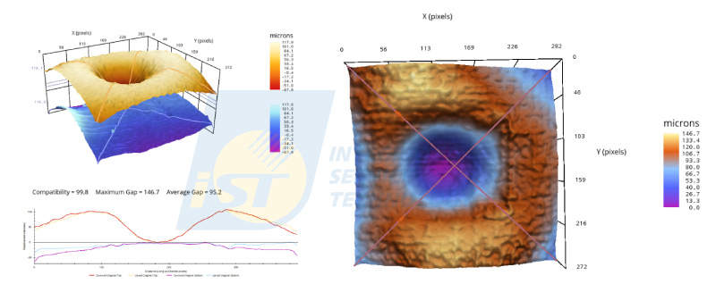
Figure 8: Overlaying 3D data from ICs and PCBs allows for precise warpage visualization and quantifying gaps, helping identify misalignment or potential warpage zones.
(Source: iST)
These advanced surface metrologies can be used independently or in combination. For complex heterogeneous structures such as CoWoS and Fan-Out, iST lab recommends pairing WLI + AFM or 3D Profiler + Shadow Moiré for comprehensive area and detail analysis.
In the face of evolving demands from AI chips, HPC, and advanced packaging, choosing the right measurement tool directly affects development efficiency and yield.
We hope this iST Tech Classroom article has provided deeper insight into surface morphology analysis. Thank you for your continued support. To receive a comparison table of these four advanced tools, contact us at marketing_tw@istgroup.com.
Relevant engineering inquiry please contact Mr. Andy Chang at 03-579-9909 ext. 6436 or via email at web_BLR@istgroup.com.