Issued Date:2024/4/16 Traces of dislocations
Issued By:iST

During the chip manufacturing process, dislocations pose a significant challenge as these minute defects can lead to leakage currents in semiconductor devices, thereby severely impacting their reliability. TEM is currently the only analytical tool capable of observing these nanoscale dislocations. However, harnessing its full power requires considerable technical expertise and knowledge. Would you utilize TEM, this superlative tool, to analyze the traces of dislocations? Let’s unlock more TEM techniques together today!
Traces of dislocations
Previously, we mentioned that the first category of semiconductor materials includes Silicon and Germanium. Due to mature wafer refining techniques, the density of dislocations in Si wafers for semiconductor device fabrication approaches to zero, typically consisting only of vacancy defects in zero-dimensional space, while the concentration of dislocation defects in one-dimensional space is nearly zero.(Read more: Decoding GaN Epitaxial Layer Dislocation Types with TEM Analysis) However, dislocations are induced when improper annealing process was used during ion implantation process. A dislocation penetrating p-n junctions will become a leakage path and reduce the reliability of this semiconductor device.
TEM(Transmission Electron Microscopy)/STEM(Scanning Transmission Electron Microscopy) is the only nano material analysis technique that can observe dislocations. The type and the density of dislocations can be characterized by TEM/STEM images at specified diffraction conditions [1 ~ 3]. Moreover, TEM 3D imaging techniques can trace dislocations inside crystals [4 ~ 6].
This article will explore how to use TEM 3D imaging techniques to analyze the extension traces of dislocations within the silicon substrate of semiconductor devices. For semiconductor devices prone to leakage failures, analyzing the extension traces of dislocations is a critical aspect of TEM analysis.
Traces of dislocations
Traces of dislocations
1. Introduction of TEM 3D Imaging Techniques
Functions of current TEM/STEM are powerful, a TEM/STEM system has more than ten micro-nano material analysis techniques available. Among them, there are three techniques can analyze the 3D trace of dislocation in the crystal. They are TEM tomography [5, 6], 3D TEM, and TEM stereo [1, 3].
(1) TEM tomography
TEM tomography is the most advanced one, but its operation is complicated and time consuming, so it is adapted in TEM laboratories of academic and research institutes, but not in industrial ones, and the range covered by the sample is usually too narrow.
(2) 3D TEM:
Plane-view type TEM specimens were usually used for TEM observation firstly, then adequate protection layer was coated on the region containing dislocations, finally one more FIB cutting was conducted. This takes some risk of destroying the TEM specimen and getting rid of parts of dislocations, and gives improper data.
(3) TEM stereo:
On the other way, TEM stereo needs one TEM specimen only, photo dislocations from two orientations of same diffraction condition, then do some basic geometrical measurement and calculations, the trace of dislocations can be descripted. The method is much simple for TEM sample preparation and has higher yield.
2. Sailboats Far Away from the Coast
It is hard to judge which one is farther when two sailboats are far away from the coast, as shown in Figure 1. The distances of them from the coast can be calculated by using basic geometry if a large flat region is available. Figure 2 is a top view schematic diagram of Figure 1. The observer travels a distance L parallel to coast, the LA and LB are distances between sailboat A and sailboat B to the observer respectively, and θA and θB are corresponding angles of sailboats to the two ends of the L line. The values of LA and LB can be calculated to be a certain accuracy when a protractor and a ruler of certain accuracy are available.
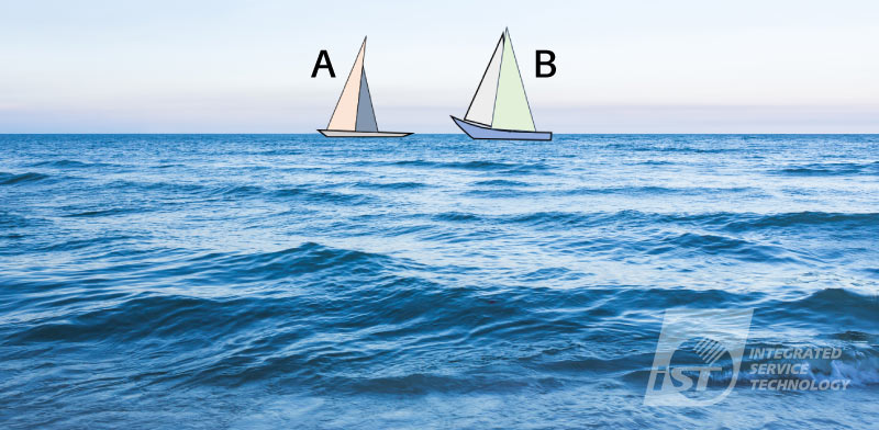
Figure 1: Two sailboats far away from the coast.
(Source: iST)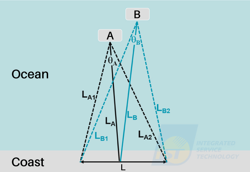
Figure 2: A top view schematic diagram of Figure 1.
(Source: iST)3. Depth of Field of TEM Images
The ray diagram of a simple thin convex lens is shown in Figure 3. The yellow arrow at the left side stands for the object, and the blue arrow at right side stands for the magnified upside-down real image on the imaging plane. For a fixed image plane, the depth of field (DOF), Dfd, is the total distance the object moves forward and backward while the image is still in acceptably sharp focus. For a fixed object, the depth of focus (DOS), Dfs, is the total distance over which the image plane can be displaced while the image is still in acceptably sharp focus. α is the angle between the optical axis and the line connecting the center point of the object (or image) and periphery of the lens. Both DOF and DOS are functions of α and the resolution of the lens, d. Generally, DOF and DOS are 400 nm and 1000 m respectively for a TEM operated at 200 KeV. The large value of DOF means that features in the specimen, from top to bottom, are all in focus. So, the relative depth of two features is not able to be identified from a single TEM image, as blue line and yellow line described in Figure 4(a).
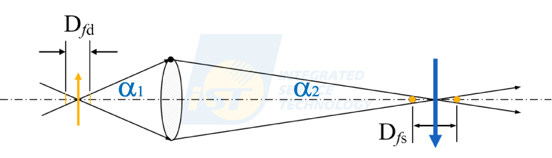
Figure 3: The simple ray diagram of a thin convex lens.
(Source: iST)The corresponding structure of the schematic projected image of Figure 4(a) can be either Figure 4(b) or Figure 4(c). It means that the 3D structure is unable to be determined from a single image such as Figure 4(a). If we tilt the specimen counterclockwise, as Figure 5(a), and the spacing between yellow and blue lines increases, as shown in Figure 5(b), then we can deduce that the 3D structure is that shown in Figure 4(b), not that shown in Figure 4(c).
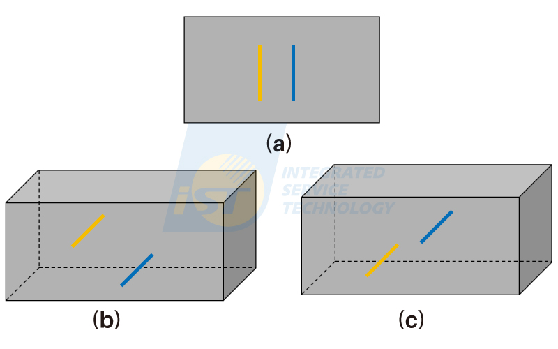
Figure 4: Schematic diagram of an image and possible crystal structures. (a) Schematic TEM BF image, (b) schematic crystal model with yellow line above and blue line below, (c) schematic crystal model with blue line above and yellow line below.
(Source: iST)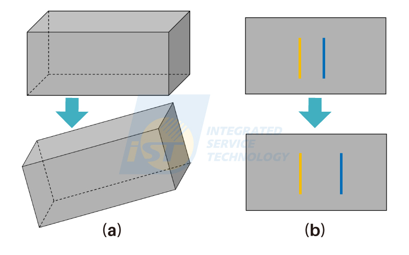
Figure 5: Illustration of specimen tilting(a) and corresponding image change(b).
(Source: iST)4. Traces of Dislocations In Crystals
Dislocations do not terminate in the crystal unless they form loops. So, dislocations induced in silicon substrates due to improper annealing heat treatment after ion implantation will run through the silicon crystal. They will become leakage paths if they penetrate the p-n junctions.
Traces of dislocations in a TEM specimen can be characterized by specimen tilting similar to that shown in Figure 5(a). Because atoms of dislocations are all silicon, same to matrix around, diffraction contrast of TEM images with dislocation is the dominating image contrast mechanism. Thus, morphology of dislocations changes with diffraction conditions. Dislocations can be invisible at some diffraction conditions. Two beam diffraction conditions with optimum deviation parameters should be used to analyze dislocations. Two images taken at two angles separating 15 ~ 20 degree should be kept at same two beam condition, so the change in morphology of dislocations can be minimized.
A set of typical TEM stereo images are shown in Figure 6. Two dislocations labelled A and B in a TEM BF image taken at [100] exact zone diffraction condition, as illustrated by the CBED pattern inserted at the lower right corner, is shown in Figure 6(a). Figure 6(b) and Figure 6(c) are two TEM BF images of same two beam condition, but about 8 degrees opposite orientation related to Figure 6(a). The distance between dislocation A and dislocation B in Figure 6(b) is distinctly smaller than that in Figure 6(c), i.e. d1 < d2. The distance, L, between dislocation A and the edge of the active region (marked by a red dash line) decreases from Figure 6(b) to Figure 6(c). Changes in distances in Figure 6(b) and Figure 6(c) are similar to that described in Figure 5. So, we can deduce that dislocation A and dislocation B locate at different depth at first glance.
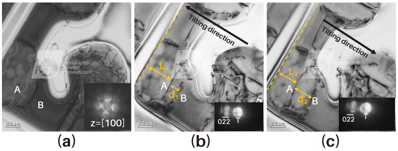
Figure 6: TEM BF images of different diffraction condition show changes in morphology and relative positions. (a) [100] exact zone, (b) 0 -2 -2 two beam condition, orientation 1, (b) 0 -2 -2 two beam condition, orientation 2. Ref.[7]
(Source: iST)By using the edge of the active region to be a reference line, data of distances of some inflection points of dislocation A and dislocation B are measured. The traces of dislocations, as shown in Figure 7, of these two dislocations can then be depicted after some basic geometry calculation. Dislocation B runs in surface layer only, but dislocation A extends down to 260 nm. This means that dislocation A penetrated p-n junction and formed a leakage path which caused a leakage fail in this device.
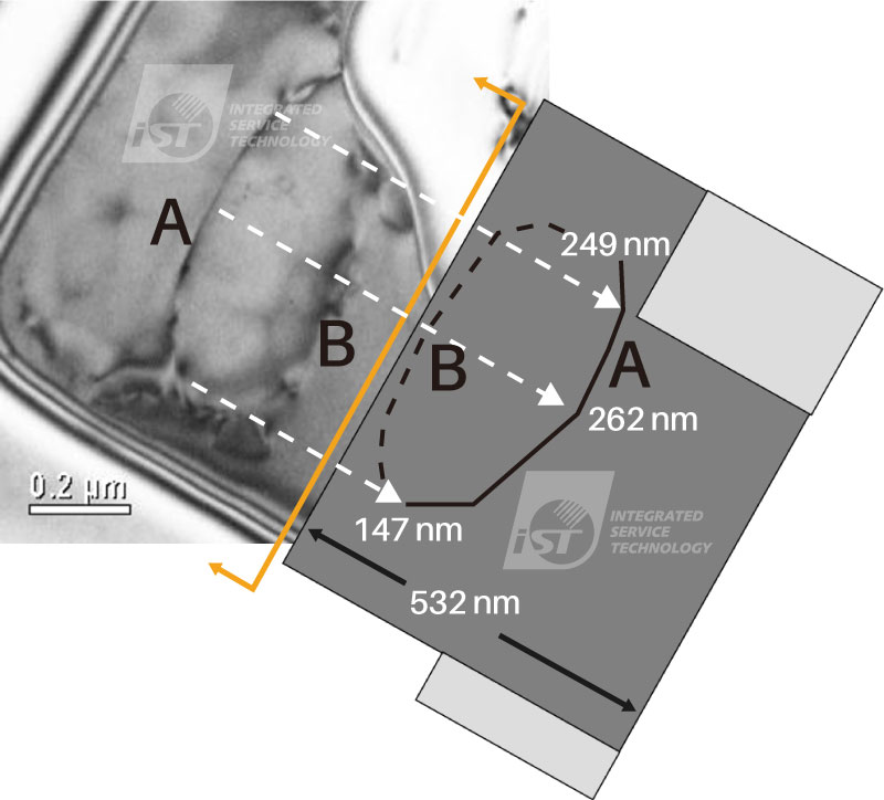
Figure 7: Traces of dislocations. Ref.[7]
(Source: iST)
TEM is the only micro-nano material analysis technique that is able to analyze crystal defects, such as dislocation etc., in crystalline materials. Besides morphology, density, and type, TEM can further analyze traces of dislocations in silicon substrates and determine whether they penetrate the p-n junction to form a leakage path. If we can fully utilize the capabilities of TEM, we can gain a more comprehensive understanding of the material’s microstructure and properties, thereby enhancing our ability to analyze component failure.
iST’s Material Analysis Laboratory has extensive experience and successful cases in the semiconductor process and advanced packaging fields. In this article, we share this knowledge with our long-time supporters. If you have related needs or would like to further understand this knowledge, please feel free to contact marketing_tw@istgroup.com
References:
[1] J. W. Edington, Practical Electron Microscopy in Materials Science, Van Nostrand Reinhold Company, New York (1976). ISBN: 0-442-22230-0
[2] G. Thomas and M. J. Goringe, Transmission Electron Microscopy of Materials, John Wiley & Sons, Inc., New York (1979). ISBN: 0-471-122440-0
[3] David B. Williams and C. Barry Carter, in Transmission Electron Microscopy, Microscopy, part 2, Plenum Press, New York (2007). ISBN: 0-471-122440-0
[4] 鮑忠興,穿透式電鏡三維立體成像術,科儀新知第三十卷第二期,48-54 (2008)。
[5] G.S. Liu, S.D. House, J. Kacher, M. Tanaka, K. Higashida, I.M. Robertson, “Electron tomography of dislocation structures”, Material Characterization, Vol. 87, 1-14 (2014)
[6] Alexandre Mussi, Ahmed Addad, Fabien Onimus, “Dislocation electron tomography: A technique to characterize the dislocation microstructure evolution in zirconium alloys under irradiation”, Acta Materialia, Vol. 213, 116964 (2021).
[7] J. S. Bow and Speed Yu, “Depth Measurement of Dislocations in Si Substrate by Stereo TEM,” Proc. ISTFA, 233-234 (2005).