Issued Date:2023/7/27 TEM DF
Issued By: iST

Did you know about the little-known yet incredibly useful feature of TEM? How to select and combine at least 8 types of image analysis techniques from TEM to achieve efficient and effective material analysis?
TEM DF
Transmission electron microscope (TEM) has been the most important instrument for nano-materials analyses since mid-twenty century. Its resolution can reach about 2 nm for analysis of images, crystalline, and composition, and even to atomic scale after 2015. TEM was divided into three groups: conventional TEM (CTEM), analytic TEM (AEM), and high-resolution TEM (HRTEM), by its main function before 1990 [1 ~ 5]。
The function and performance of current TEMs have been much better than those of TEMs of 1990. All current TEMs have STEM function and resolution power beyond 0.2 nm. Techniques of materials analyses offered by these new TEM/STEM systems are illustrated in Figure 1[6]. Any TEM, depending on the brand and optional features, will have at least eight image techniques and five diffraction techniques. EDS (Energy-Dispersive X-ray Spectroscopy) and/or EELS (Electron Energy Loss Spectroscopy) are both performed by the spectrum image technique, data of small local regions, line profiles, and elemental maps are then processed from these acquired data. How to make a best choice among these TEM techniques to proceed an effective and efficient materials analysis is an important topic.
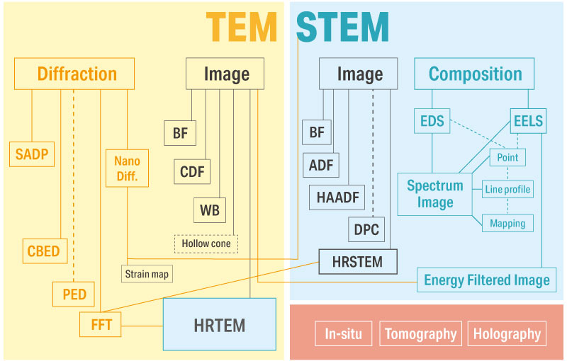
Figure 1: Typical materials analysis techniques offered by the TEM/STEM system. Techniques in the pink block are only available in some special TEM laboratories. [6]
Currently, TEM/STEM bright field images, STEM dark field images, HRTEM images, and EDS analysis are usually combined for most routine TEM analyses. TEM engineers in these TEM laboratories have become skilled operators after long time routine works. This article is not going to discuss those widely used TEM techniques mentioned above, but will discuss some TEM techniques which are not often used in present semiconductor specimens but may be used for semiconductor materials of next generations and other material systems.
TEM DF
TEM DF
1. Unveiling the Unique Abilities of the Dark Knight: TEM DF Imaging Case Studies
STEM dark field images, including ADF(Annular dark-field) images and HAADF(High-angle annular dark-field) images, are frequently used in daily TEM analyses in semiconductor industry, while TEM CDF images are usually set aside at the same time. The dominated mechanism of image contrast is different for TEM CDF images and STEM DF images. Diffraction contrast is the image contrast mechanism for TEM CDF images, and atomic number contrast is the dominated image contrast mechanism for STEM HAADF images. We will illustrate the advantages of TEM CDF images in following analysis cases.
Case 1: Nanocrystals That Are Not Clearly Visible in BF Imaging Become Distinctly Visible When Switched to TEM CDF Imaging
When the grain size of a poly crystal material is much smaller than the specimen thickness, grains in TEM BF(Bright Field) images are overlapped and hard to be outlined. This makes the work of grain size measurement difficult. TEM CDF (Center Dark Field) images use only parts of diffraction beams to form images, so only grains contributed to those diffraction beams show bright contrast, as shown in Figure 2 (b) and (c). Even though less grains are visible, grain size measurement is easy to proceed. In addition, since the composition is identical for all grains, the brightness will be same for all grains in STEM HAADF images.
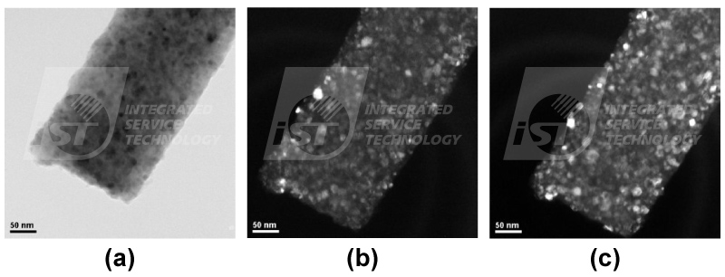
Figure 2: TEM Images of a nano crystal material. (a) TEM BF image, (b)&(c) TEM CDF images.
Case 2: Clear Visualization of Amorphous Laser Marks in TEM CDF Imaging
TEM CDF images for amorphous phases have unique advantages for some specified material systems, DVD is one of them. The recording layer in DVD is a layer of metal thin film of nano grains. Laser marks are formed when a laser beam of adequate energy scans the metal thin film. Because the reflectivity of amorphous phase and metal of nana grains for the laser beam is different, laser marks of different length are then decoded to be signals of video or data for PC when a laser bean reads them.
Figure 3 shows a set of TEM images and corresponding selected area diffraction pattern (SADP). The diffused ring in SADP pointed by a yellow arrow results from the amorphous phase in DVD. Other rings with defined width and larger diameter in the SADP are diffraction rings of those nano metal grains. The smallest OBJ (Objective) aperture, as depicted by the yellow circle in Figure 3(b), was selected to let those limited electrons, including some of the first ring (diffused) and some of the second ring, pass through to form the CDF image shown in Figure 3(c). Bright phases in this CDF image can be divided into two kinds: white nano grains and grey laser marks. Nano grains will show bright contrast when their corresponding diffraction electrons passing through the OBJ aperture and show dark contrast when their corresponding diffraction electrons blocked by the OBJ aperture. All amorphous laser marks show grey color and have almost same brightness level. Contours of laser marks in Figure 3(c) are more distinct than those in Figure 3(a) due to the image contrast.
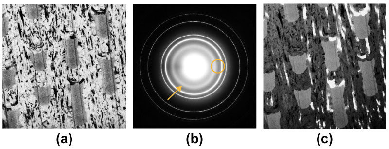
Figure 3: TEM analysis of DVD recording layer. (a) BF image, (b) corresponding SADP, (c) CDF image.[7]
Case 3: Identify Amorphous Phases through Material Distribution Using TEM CDF Imaging
Amorphous phase in as-deposited BaTiO3 thick film deposited by aerosol deposition was characterized by X-ray diffraction (XRD). This amorphous phase was transferred to the crystalline phase after high temperature annealing. TEM BF images told that most grains were smaller than 50 nm, but was not able to characterize the distribution of amorphous, homogeneous? or localized?
The diffusion ring (pointed by the green arrow in Figure 4(c)) corresponding to the amorphous can be dimly observed in the SADP, while it was not detected in the annealed specimen. The TEM CDF images shown in Figure 4(b) showed a foggy zone which distributed among nano grains. We deduced that a few of amorphous BaTiO3 distributed among grains homogeneously in the as-deposited BaTiO3 thick film. It means that the grain boundaries are amorphous phases for the as-deposited sample.
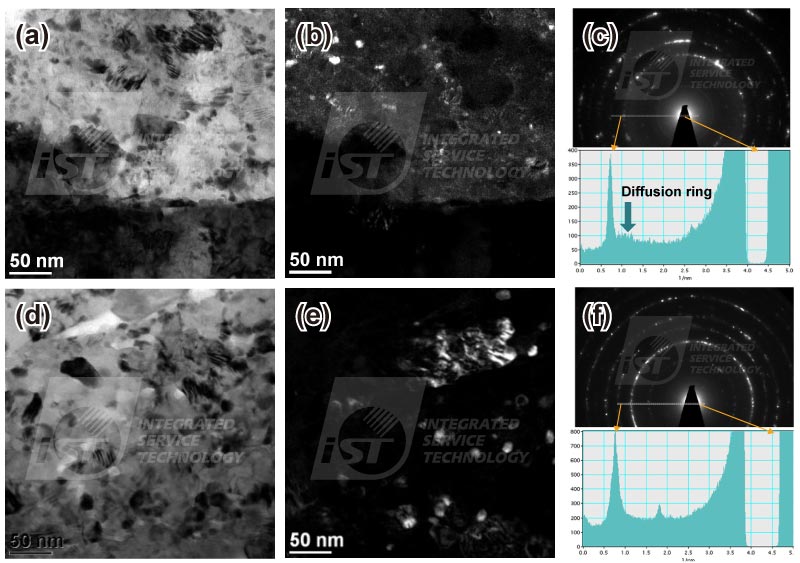
Figure 4: TEM BF images, CDF images, and SADPs of aerosol deposited BaTiO3 thick film. (a)(b)(c) as deposited, (d)(e)(f) after thermal annealing.
Case 4: Analyzing Material Orientation Structure through Hollow Cone of Shadows in TEM Central Dark-Field Imaging
Some materials have a textured structure, such as wood texture. Mechanical properties and physical properties of textural materials are anisotropy. Grains of steels elongate along the rolling direction and a specified group of crystal planes, {h1 k1 l1}, are parallel to or nearly parallel to the surface of the steel after cold rolling to reduce the total energy of this kind of materials. In nature, the grain size of Hetian jades falls in the range of nano scale and has a texture structure, as shown by the TEM BF image (Figure 5(a)). The grains are approximately lenticular with long axes of 300 to 600 nm and short axes of 50 to 100 nm. The long axes of most of these lenticular grains run along a specified direction instead of random orientation, as shown by the BF image and SADP in Figure 5(a). An optimum OBJ aperture (indicated by the yellow circle in Figure 5(a) SADP) is selected to allow some diffraction electrons to pass through to form a CDF image shown in Figure 5(b). Some grains along this aligned direction show bright contrast in the CDF image. When the CDF image formed by the hollow cone (HC) technique [8, 9], all grains along this aligned direction show bright contrast as shown in Figure 5(c).
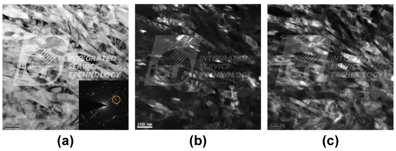
Figure 5: (a) TEM BF image, (b) TEM CDF image, (c) TEM HC image, of a Hetian jade.
The HC image is a special technology of TEM CDF images. Every group of crystals of copper with crystal planes {111}, {002}, {220}, etc. perpendicular to the incident beam. can be viewed separately and simultaneously by using HC images properly, and sets of data are analyzed to determine the material having preferred orientation structures or isotropic structures. This kind of materials analysis in Cu materials is very important in field of 3D IC and multilayer PCBs (printed circuit boards). They are analyzed by EBSD (Electron Backscatter Diffraction)(Read more: Crystal Structures in Materials: The Key to Unbeatable Semiconductor Advanced Packaging) currently, and TKD (Transmitted Kikuchi Diffraction) for grain size smaller than 50 nm. It is predicted that HC images have to be used for analyzing Cu materials with grain size smaller than 20 nm.
2. Extracting the Essence, Sharing Examples of Fourier Filtering in HRTEM Imaging
In addition to the four cases mentioned above that optimize material analysis using CDF imaging in TEM, the following will introduce a combined application case of TEM – utilizing HRTEM in conjunction with Fourier filtering techniques to improve image quality.
Critical Dimensions of some key structures in semiconductor devices, such as gate oxide (GOX), quantum well (QW), etc., are several nano meters to several tens of nano meters only. The dimension of these key features needs image techniques with resolution power better than 0.2 nm to provide good accuracy. After careful alignment, all modern TEMs can go into the HRTEM mode and provide atomic-level resolution.
The first requirement to obtain high quality HRTEM images is that the specimen thickness must thin enough, falling in the range of 20 to 60 nm. The effect of chromatic aberration, increasing with the specimen thickness, will make HRTEM images blurred, resulted from more noise of high frequency between atoms, as shown by the left HRTEM image in Figure 6. The easiest way to improve the quality of this blurred HRTEM image is to use Fourier filtered technique. As shown in Figure 6, a Fourier transfer pattern of the blurred HRTEM image is taken first, then a built-in array mask is applied to this pattern. After applying the aligned mask to keep diffraction spots and filter out noise between spots, an inverse Fourier transfer is calculated, and a Fourier filtered HRTEM image, as shown by the right HRTEM image in Figure 6, is obtained. A significant difference in clarity of atoms between these two images is observed.
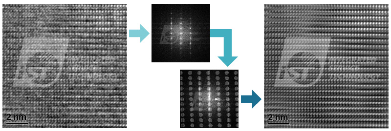
Figure 6: Typical process of HRTEM Fourier filtering. A set of FFT pattern is first transferred from the HRTEM, an array mask is then applied to this FFT pattern, a Fourier filtered HRTEM image is finally obtained.
It is very important to set a group of correct masks in the process of Fourier filtering. Some fine structures will be filtered out with an improper mask setting, this makes the filtered HRTEM image be unsuitable to represent the original HRTEM image. There is a crystal defects of plane type (or a second phase) of about 3.3 nm in the HRTEM image shown in Figure 7(a). This planar crystal defect has three bands, each band is consisted of only three atom layers (~ 1.0 nm). Besides diffraction spots, streaks extending from diffraction spots and running along a direction perpendicular to the planar defect in the FFT pattern of this HRTEM image are observed. If using one set of array mask to cover those diffraction spots (Figure 7(e)) only, the filtered HRTEM image will be the one shown in Figure 7(b). Obviously, the boundary of the planar crystal defect, as marked by two white arrows, is invisible in this filtered HRTEM image. Adding two more sets of masks to include those streaks (yellow and white arrows in Figure 7(f)), the filtered HRTEM image will be the one shown in Figure 7(c). Fine structures in this HRTEM images are kept.
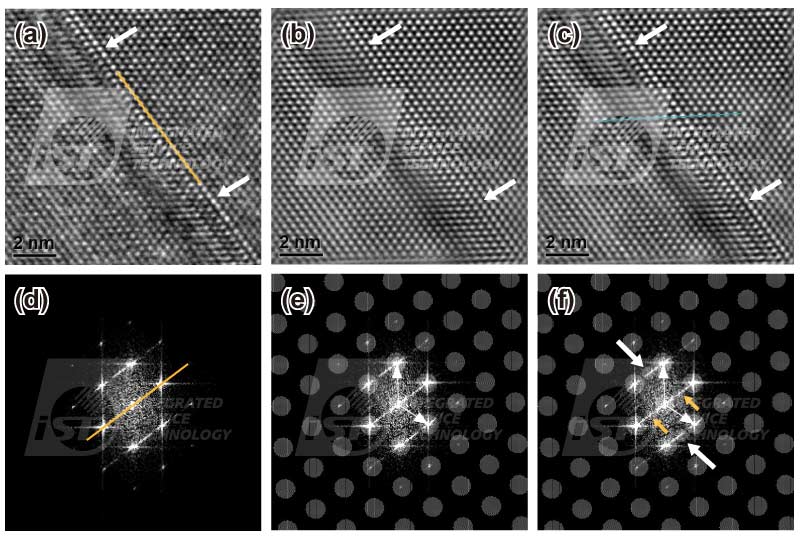
Figure 7: A HRTEM image with a planar crystal defect inside. (a)the original HRTEM image and (d) the corresponding FFT pattern of (a), (b)the Fourier filtered HRTEM image using an array mask only and (e) the corresponding FFT pattern of (b), (c)the Fourier filtered HRTEM image using a set of composite masks and (f) the corresponding FFT pattern of (c).
Four different types of applications of TEM CDF images and an example of Fourier filtered HRTEM image are illustrated in this article. They solved different material problems. Combined with those mostly used TEM techniques: TEM/STEM BF image, STEM DF image, HRTEM image, and EDS analysis, services of TEM materials analyses by iST will cover a wider range of material systems in this field, and are always effective and efficient.
Due to the limit of medical resource and economic issue, people usually take only necessary examinations when they go to hospital for medical treatment. TEM analyses performed in semiconductor industry are basically for process tuning, so only some techniques listed in Figure 1 are selected for each specimen.
iST Material Analysis Laboratory has been working in the semiconductor and advanced packaging fields for a long time and has accumulated considerable experience and successful cases. Should there be any inquiry or if you would like to know more about the aforementioned techniques, just email us web_ma@istgroup.com or marketing_tw@istgroup.com。
References:
[1] David B. Williams and C. Barry Carter, Transmission Electron Microscopy, Microscopy, part 1, Plenum Press, New York (2007).
[2] J. W. Edington, in Practical Electron Microscopy in Materials Science, published by Van Nostrand Reinhold Company, New York (1976).
[3] Joseph I. Goldstein, in Practical Scanning Electron Microscopy, edited by Joseph I. Goldstein and Harvey Yakowitz, Plenum Press, New York, 3rd edition (1977).
[4] Gianluigi Botton, “Analytical Electron Microscopy” in Science of Microscopy, edited by Peter Hawkes and John C. Spence, Chapter 4, 273-405 (2007).
[5] John C. H. Spence, High-Resolution Electron Microscopy, 2nd edition, New York, Oxford University Press, Inc. (1988).
[6] 鮑忠興,淺談TEM分析上常見的主要困惑,科儀新知(2022)。
[7] 鮑忠興和劉思謙,「近代穿透式電子顯微鏡實務」,第二版,台中,滄海書局(2012)。
[8] J. S. Bow “Analysis of Co-deposited Ti-Hf Thin Film on (0001)6H-SiC by HRTEM, Energy-selected and Hollow Cone Images,” Proc. Micro. Soc. Amer., 978-79 (1994).
[9] Chun-Ying Tsai, Yuan-Chih Chang, Ivan Lobato, Dirk Van Dyck & Fu-Rong Chen, “Hollow Cone Electron Imaging for Single Particle 3D Reconstruction of Proteins,” Scientific Reports, Vol. 6, 27701 (2016).