Issued Date:2023/3/7 IC Assembly
Issued By:iST
The schedule of low-volume engineering samples has been delayed because the capacity in large OSATS is occupied by mass produced ICs. How can I get the assembly resources to proceed on schedule?
In the R&D stage, after wafer prototypes are ready, most of them must be assembled for the following engineering verification.
Recently, iST has noticed that more and more customers, especially academic and research institutions, are seeking quick assembly of engineering samples in addition to engineering verification requests.
The main reason for this phenomenon is that the capacity of large assembly factories is fully occupied by mass-produced parts, and therefore, they are unable to accommodate orders for low-volume engineering sample assembly.
To provide engineering packages to customers as well as academic and research institutions, iST established a quick assembly lab 20 years ago. Every year, it produces hundreds of thousands of prototype ICs for the experimental engineering packages of semiconductor companies as well as academic and research institutions.
This iST classroom is presenting you how the iST quick assembly lab works to provide engineering packaging samples in time, especially focusing on how quick assembly services overcome sample preparation’s testing bottlenecks of special packages, including SiP (System in Package), MCM (Multi Chip Module) and QFN (Quad Flat No-Lead).
IC Assembly
IC Assembly
1.iST reference COB package for fast engineering sample delivery.
Chips by mass production are conventionally packaged with a lead frame and the substrate by a process with 20-30 steps lasting 3-14days. The iST’s quick assembly lab has simplified this process to just 4 steps (Figure 5) through the ceramic (Figure 1), plastic pre-mold (Figure 2) and reference COB/Socket (Figure 3, Figure 4) provided.
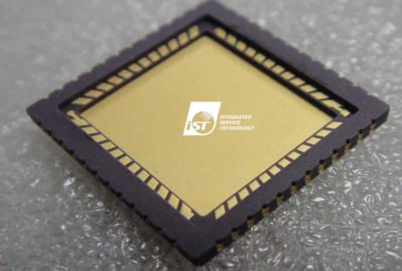
Figure 1: Ceramic substrate

Figure 2: Plastic pre-mold
What we want to stress here is that currently, most chip packages need to go through wire bonding verification, so iST COB features a common and integrated testing environment to support packages like 48/64/256-pin (Fig. 3 and 4), and completes samples quickly and easily for fast function analysis.
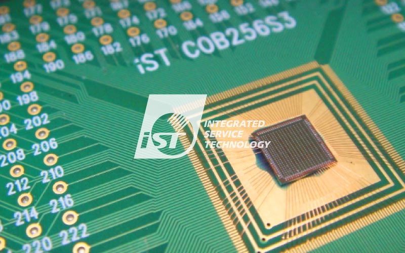
Fig. 3: PGA256 wire-bonding COB
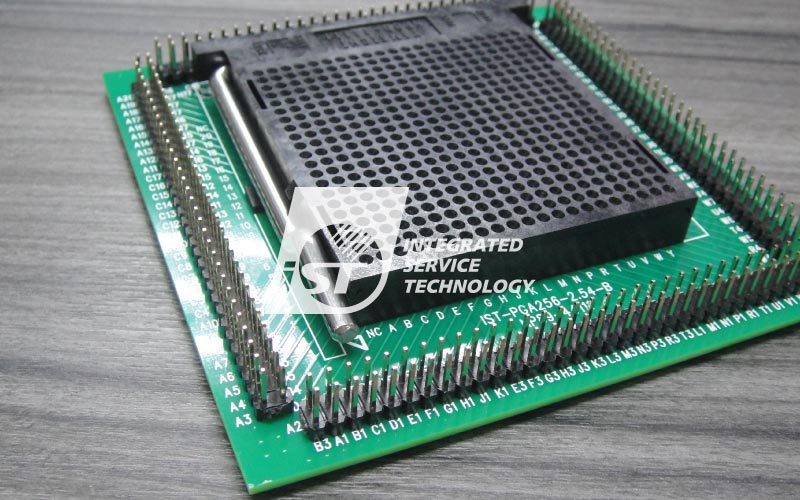
Fig. 4: iST COB test socket and socket board
First of all, validate the wire bonding diagram: you may provide iST with the diagram by the assembly house or have iST prepare it and select the materials needed based on chip data you provided. iST will start making official samples once the layout gets validated. The next step is to mount dies on packaging materials with conductive or non-conductive adhesive before bonding them with the required wires and given wire diameter per specifications of the chip.
Addressing customer’s test or use methods, iST may deliver the packaging samples for engineering verification with the chip and wire protection by glass or, ceramic cap or sealants provided by iST.
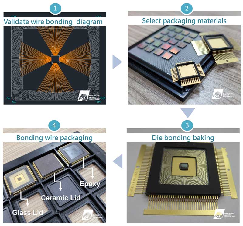
Figure 5: Quick assembly in just 4 steps
2. An ace in the hole of multi-chip packages’ verification: IC repackaging technology
To identify failure of the single component which results in defective IC is a tall order. Internal wiring and board circuit connections among SiP, MCM, MCP, and QFP tends to suffer in electric tests by interference of other chips or device components which, in turn, makes test results hard or even impossible clear.
An unique solution of IC repackaging developed by iST allows customers to remove the die for inspection from packages like SiP, MCM, MCP or BGA. With using the substrate provided by the customer (Fig. 6 e) or tailored by iST (Fig. 7),and then, the lab processes dies and wire bonding (Fig 8), molding, trimming and ball mounting (Fig 9) to repackage into specific packages requested by the customer for subsequent electrical tests. (Further reading: IC Repackage Ease-up Inspection Over Advanced Chip Packaging)
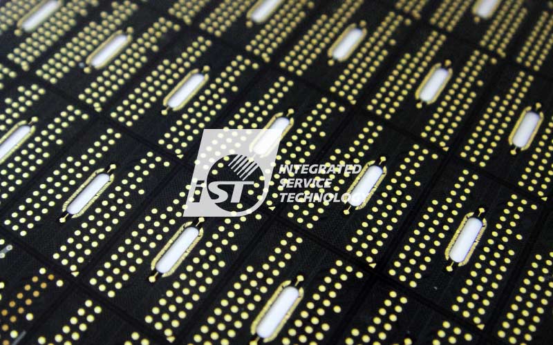
Fig 6: Dedicate BGA substrate from customer
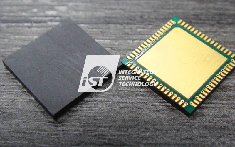
Fig. 7: Custom QFN PCB
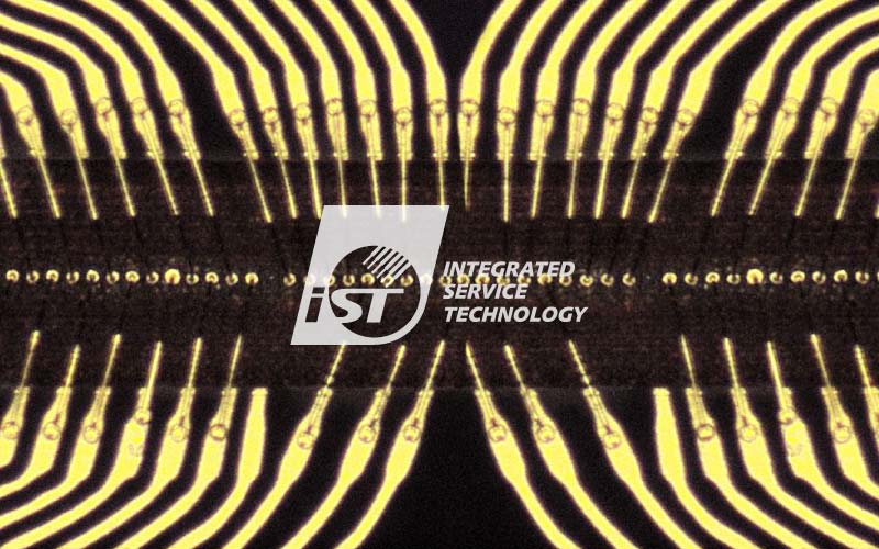
Fig. 8: Die attach and wire bonding
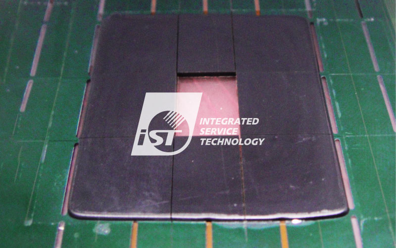
Fig. 9: Molding and sawing
3. How to process engineering sample preparation with complex package designs?
It is necessary to process samples for test before reliability test or failure analysis during R&D stage.That is, the technology applied to sample preparation plays a critical role in determining if the following functional test is accurate and if defects can be easily located.
In traditional sample preparation, IC decapping and front-size polishing are the most commonly-used approaches; the operator decaps the front of packages by chemicals or laser, or grinds the back of molding to expose the chip, or like mentioned earlier, conducts sample preparation by removing the die for repackaging.
However, the increasing complexity of package wires raises risks of re-bonding wires. The bond pad in original packages becomes more fragile after chemical etching and this also forces the following failure analysis to rely on the backside for more clarity because the chip consists of too many layers.
iST quick assembly lab can help you remove the substrate impeding back observation and lead wires of solder joints of specific locations by bridging, and then acquire the accurate defect location from the backside through EFA analysis.
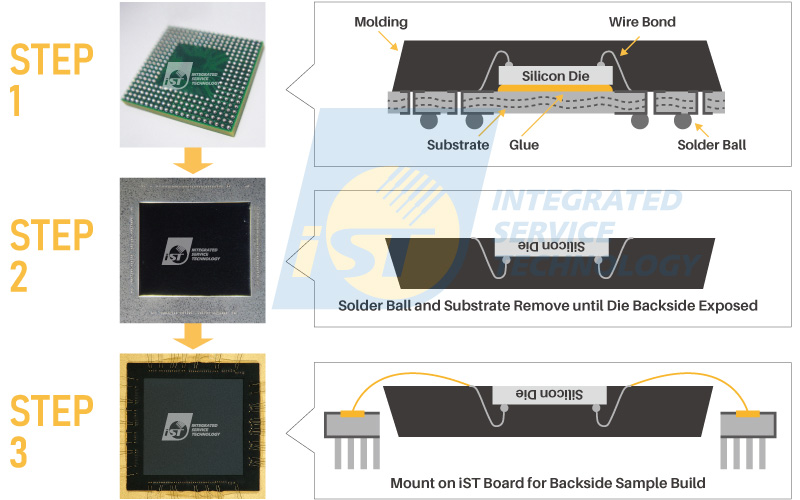
Fig. 10: Remove back substrate and lead specific wires
This is to share knowledge and experiences of iST with you. In addition to quick assembling, iST lab provides services for wafer sawing, die attaching, wire bonding, etc. An One-stop Solution based flip chip packaging service aligned with your chips and tailor-made substrate also provided for you to enable ESD, OLT and reliability analysis and shorten the preparation time of samples under test effectively. Should there be any inquiry or if you would like to know more about the aforementioned techniques, just ring Mr. Peter Chen at +886-3-579-9909 Ext. 6861 or email him at ist_assy@istgroup.com;marketing_tw@istgroup.com
Other services you may be interested in
IC Assembly