Issued Date:2022/1/5FT Socket
Issued By:iST
Do you feel trapped when you need to package a small amount of chips for testing yet no assembling and testing houses would offer their help?
When market-available ceramic packaging materials fail to work as the required testing socket, what can you do?
The last step before delivering chips for packaging is to subject finished wafers to chip probing (CP) to screen out defective chips. Bare chips successfully tested then can be packaged and delivered to customers after successfully going through the final test (FT).
There is a catch here. Most newly developped or customer returned chips come in small quantities. This made their packaging take a longer time to go through the assembly houses’ production line or directly rejected by their order taking window.
You may laugh at the situation as an easy option, embedding chips with ceramic packaging materials has long been adopted by the industry.
The problem with the latter is that they can only partially meet the needs of FT. Market available single-spec ceramic packaging materials may fail to provide pins of width and length required by test socket/carrier. Their substances (ceramic) are totally different from the plastic one employed by the plastic pack body and may hamper the FT results.
iST knows your sorrow. This iST Classroom is designed to tip you to decap existing IC finished goods on hand into test socket/carrier for easy and effective FT later.
FT Socket
1. Decap Existing IC Finished Goods into Test Socket/Carrier
Step 1: Choose one finished IC that fits your test socket/carrier; decap it to expose its wires and chip body (Figure 1) for removing them later.
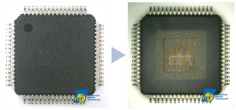
Figure 1: Exposed chip body and some bonding wires after the finished IC is decapped
Step 2: Remove chip body and bonding wires with physical means manually (Figure 2) to expose the substrate and lead frame (2nd bond) with the silver coating layer remaining intact
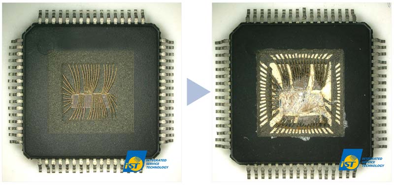
Figure 2: Remove chip body and bonding wires by iST exclusive decapping measures
Step 3: Remove residual adhesives and wires/leads left in the pack body; make sure that none of them have been left in there or it may fail to successfully function as a test socket/carrier (Figure 3).
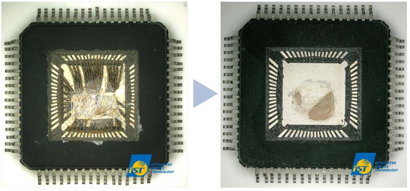
Figure 3: Package body ready for packaging and bonding
2. Combine the Sample Chip Under Test and the Test Socket
Die bond the sample chip under test in the test socket; bond required wires; protect and isolate bonding wires and the chip with encapsulation and ready the finished goods successfully.
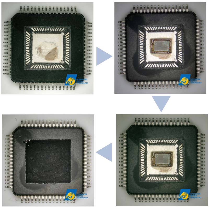
Figure 4: Combine the sample chip for testing and the test socket with die bonding, leads and sealant
In case you have any needs in making packaging materials or want to learn more about what it is all about, please call iST’s Decap department at +886-3-579-9909 Ext. 6731/6721 or Assembling department at Ext. 6870. Email: web_decap@istgroup.com .
Other services you may be interested in
FT Socket