Issued Date: 2021/5/11Wide-Bandgap-SiC-GaN
Issued By: iST
Debuted in 2021, what exactly is the WBG (Wide BandGap) that focused by leading foundries?
Amid booming 5G and electrical vehicle (EV) industries, why is the WBG being targeted by big leaders?Wide-Bandgap-SiC-GaN
After Si of the first generation and GaAs the second, the key material for making semiconductors has come to the third one’s SiC and GaN.
Wide-Bandgap-SiC-GaN
The Compound Semiconductors with WBG(wide bandgap) are looming the industry with their advanced material in 2021. What is WBG? What features it has? Why is it so loved in the coming era of 5G, EV, renewable energy, and industry 4.0?
You’ll be outlined with WBG in this iST Classroom.

1. Why is WBG Required Now?
Amid increasingly serious environment protection issues caused by global warming and carbon emissions these days, human beings are developing in the directions of energy saving and carbon reduction. This requires replacing petrochemical energies with green ones and adopting power saving practices quickly as well as pursing high energy efficiency and low energy consumption in daily life.Wide-Bandgap-SiC-GaN
Take example. The Paris Agreement worked out by the United Nations Framework Convention on Climate Change has set to keep the global warming up to 2℃. Even if we can meet this target, the world is deemed to add another 21% of CO2 emission and consume another 50% of electricity in 2050 to maintain the same standard of living as of today. It’s clear that we have to advance and improve existing energies as a result of this.
The first generation material, Si-based wafers, of semiconductor is too close to its physical limits to raise power, reduce heat loss, and increase speed. That is, Si-based wafers have to give way to those with better electron transmission efficiency and low energy consumption. This makes WBG semiconductors, featuring higher energy efficiency and lower energy consumption, the second to none choice.
2. What is a Bandgap?
Let’s begin with an outline of bandgap.
In terms of quantum physics theories, there are two bands: the one is the Valence Band (VB) and the high energy Conduction Band (CB). A BandGap (BG) is a difference of energy in between the two (see Figure 1).
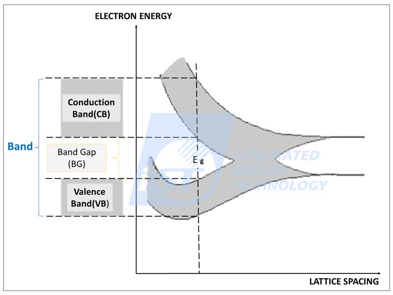
Figure: Schematic diagram of Semiconductor and bandgap (Courtesy of iST)
Metallic materials’ conduction is a result of free electronics in CB. Electronics of semiconductor materials do not flow in room temperature as they are trapped in VB and become conductive only when electrons there are transited into CB by being heated or applied with energies greater than BG.
Transistors in integrated circuits can switch on or off power when being applied with a current of small voltage. That’s why the Si materials featuring relatively smaller BG are adopted in the markets for such a long history.
This is not the case when operating temperature went above 100℃ as the Si-based semiconductors tend to deteriorate or even fail. This, in turn, prevents them from functioning successfully in demanding operation environment such as transport, military, or space tools. This drives the seeking for the WBG materials for highly voltage- and temperature-resistant applications.
It’s well known that power is proportional to the product of current and voltage. The first generation semiconductor material for power devices, Si, features a BG at 1.12eV and the second generation material for communication, GaAs, at 1.43eV have been servicing us for two or three decades. These low BG materials have to be replaced by their next generation rivals as they have hit the wall of applicability in terms of temperature, frequency, and power.Wide-Bandgap-SiC-GaN
The WBG material comes with improved operating voltage, greater power, lower energy loss, and much smaller dimension.
3. WBG Materials Available Now
There are some WBG materials available now. The SiC, a compound of Si and C, based materials come with BG over 3.0eV while the GaN and Ga2O3, a compound of Ga, N and O, up to 3.4eV and 4.9eV respectively. The diamond outruns them at 5.4eV (Table 1).
Table 1: Physics of semiconductor materials
Characteristics Si SiC(4H) GaN Ga2O3(β) Diamond Eg (eV) 1.1 3.3 3.4 4.9 5.4 Electron mobility(cm2/Vs), 1400 1000 1200 300 2000 Breakdown field (MV/cm) 0.3 2.5 3.3 8 10 Thermal conductivity (W/cmK) 1.5 4.9 1.3 0.14 20 (Courtesy of iST)
Regarding GaN and Ga2O3, in spite of being used for LED lighting or filter source of UV, them remains a tall order due to their unique characteristics.
Take example. It’s much harder and time consuming to make SiC single crystal ingot than that for Si one, let alone to deal with the dislocation defects caused by mismatched crystal lattice between GaN and silicon wafers. Both result in troublesome and costly process development.
4. Which Products are Using WBG Materials?
Global leaders, including ST Microelectronics, Infineon, and Rohm, are making huge progress in this regard. The fast chargers adopt GaN on Si or SiC substrates are now available on the markets. The high power (60W or more) GaN products on Si in addition to improved power, they come with much smaller components and more compact chargers blessed by the significantly reducing temperature and thermal effect. These fast charging applications for mobile devices and notebooks are of great potential in future.
Most existing high power products based on Si-materials are IGBT or MOSFET oriented as shown in Figure 2. It’s clear that the application range of power components and conventional IGBT modules may go over 100kW yet their speed can’t get up to 1MHz.
The GaN materials run better in speed but poor at power. Struggling with a mere power up to 1kW the latter have to be replaced with the SiC ones.
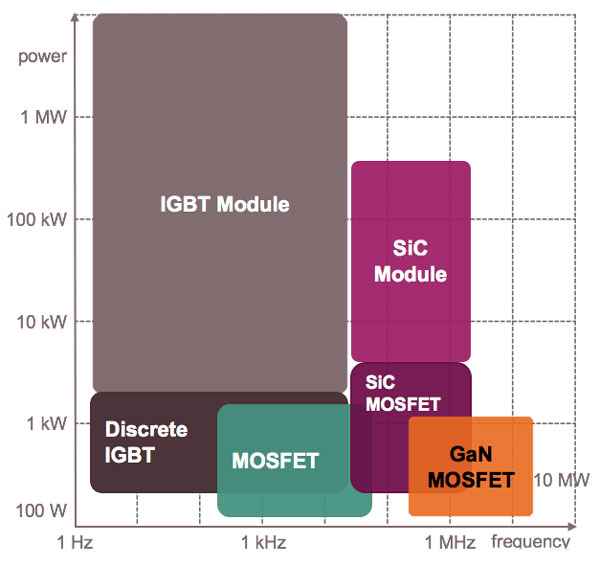
Figure 2: Application range of power components and relevant materials (Courtesy of Infineon)
Blessed by 3-folds better thermal conductivity than that of Si, the SiC may offer even smaller dimension and more competitive in the application of EVs. The IGBT originally adopted in the traction inverter and DC-to-DC converter & on-board charger by Tesla’s model 3 has been replaced by SiC power components from ST Microelectronics for better power efficiency and lower energy loss.Wide-Bandgap-SiC-GaN
Amid booming demands for powers in future, the onboard devices require not only basic high power features but also ultra-fast charging speed demanded by vehicle charging station, 5G base stations, transportation vehicles, and even satellite space stations. Relevant requirements in current transmission and conversion as well as lower energy loss will drive the large-scale development of more efficient WBG material and adoption of ultra-high power SiC components and modules.
5. Verification and Analysis in Developing and Making WBG Materials
iST has learnt that foundries and power IDMs are continuously working on the R&D of WBG materials. They need a lot of verifications in the early stage of developing new semiconductor materials. iST has been in assistance with multiple WBG suppliers for their development and production verification.
iST may prepare section samples and run dimension measurement or composition analysis (EDS) or observe with TEM over Nano-scale defects to assist suppliers in their epitaxy process relevant structure or defect analysis, to name a few.
The diffusion area relevant analysis may go with SEM observation or detection module mounted on AFM –SCM to determine type and dimension of doping area over profiled samples. See Figure 3 for an analysis over doping type in device’s diffusion area by using SEM to look into distribution of wells then determine that the upper layer comes with N- and P-well while the EPI layer the N-well.Wide-Bandgap-SiC-GaN
The iST’s SIMS may help in analyzing doping elements and concentration. See Figure 4 for analyzing a GaN on Si device’s section composition with Dual beam FIB and EDS to identify the main compositions in the epitaxial area, use it to do quantitative analysis on concentration of doping element Mg, and finally adjust electric property according to the outcome.
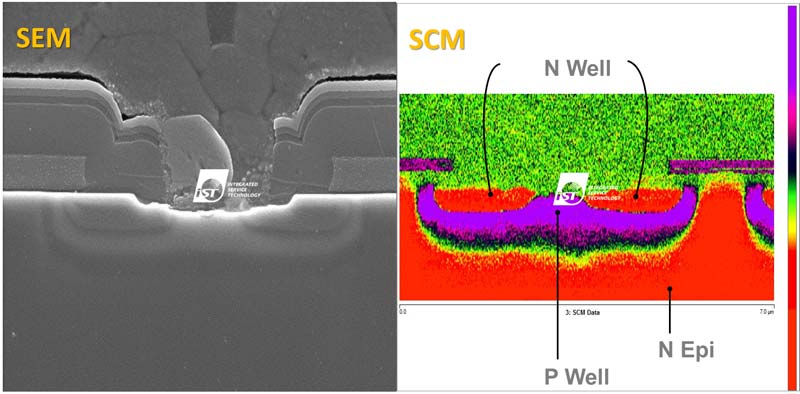
Figure 3: Use SEM to look into section structure of SiC devices, identify N/P type and measure diffusion area with SCM (Courtesy of iST)
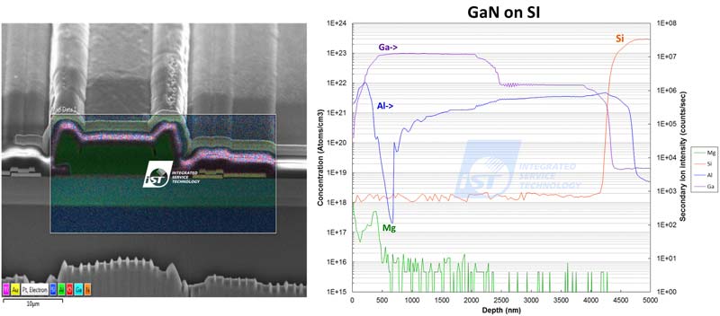
Figure 4: Use DB-FIB to look into section structure of GaN components, analyze compositions with EDS, and measure doping concentration with SIMS (Courtesy of iST)
In addition to the aforementioned WBG structure analysis services, the iST lab may deal with almost every product issues with its material analysis and failure analysis over electrical and physical properties let alone the more comprehensive verification services required by the reliability test and assessment for products mandating very high safety.
For more details, please contact iST Mr. Chang at +886-3-579-9909 Ext. 6613 or email him at sa_tw@istgroup.com