Issued Date:2020/11/03solder ball defect
Issued By:iST
Advanced packaging and heterogeneous integration is hot today
That’s the case with the quality of solder balls as well
How to identify solder ball defect quickly?
Solder ball defect

The biggest challenge faced by advanced packaging is the reliability issues caused by complex stacking of different materials in dies including warpage (see “Count Warpage Amount before SMT to Avoid Solder Empty and Early Failure“), heterogeneous materials integration and solder ball bonding.
In this classroom we’ll focus on identifying solder ball defect.
Failure analysis mandates preparing samples in advance which, traditionally, is to grind the PCB of samples with acid to remove dies for defect analysis and observation.
However, this won’t work in case of solder ball defects as the defects would be destroyed when removing the dies by grinding them with acid from the PCB. That is, any defect scene of solder balls would have long been gone by the sample preparations (Figure 1).
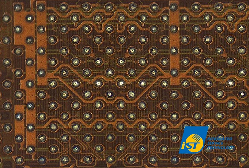
Figure 1: The solder balls are exposed after removing the die in conventional steps is very likely to hamper the scene of defects
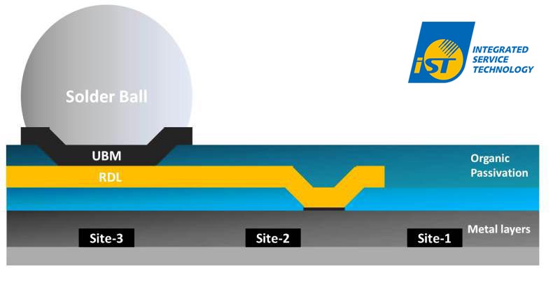
Figure 2: Structure of WLCSP
The only way to address this issue is to prepare samples from the backside as shown in the case of iST’s advanced packaging – WLCSP (Wafer Level CSP) (Figure 2). Here iST’s 3-step approach would help you in preparing samples from the backside to identify WLCSP solder ball defects quickly.
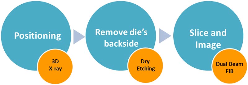
Figure 3: The three steps employed by iST to identify solder ball defects from die’s backside
Step 1: Positioning
The first step in preparing samples from die’s backside is to pinpoint the defects.
An electron microscope (i.e., OM) is used to pinpoint defects. However, inside the samples are invisible before the die’s backside was removed. Instead, an High Resolution 3D X-Ray Microscope will be used to look into the inside of samples to locate solder ball defects (Figure 4).
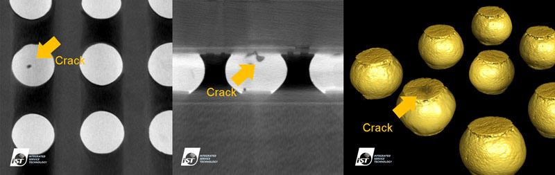
Figure 4: Cracks on solder balls found by 3D X-ray
Step 2: Remove Substrate from Die’s Backside
The next step is to remove partial or entire silicon substrate from the backside of the sample with dry etching as shown in figure 5.
The “dry etching” differs from its wet counterpart in that the former requires no acid agent at all while the latter may foil the scene of defect as the acid used may infiltrate into the defect. That is, dry etching is required for sample preparation as long as the defects are solder ball relevant.
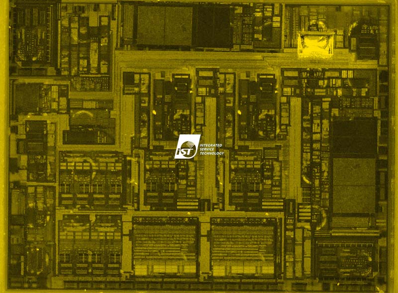
Figure 5: Removing silicon substrate by dry etching from die’s backside enable we to view solder ball distribution on the surface of WLCSP
Step 3: Slice and Image
The last step is to slice the sample with Plasma FIB or Dual beam FIB (Figure 6) and the solder ball defects displays.
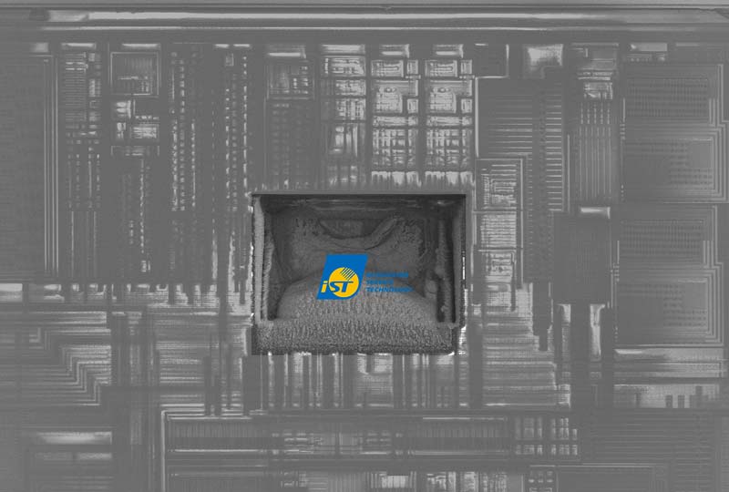
Figure 6: Slice with Plasma (dual beam) FIB
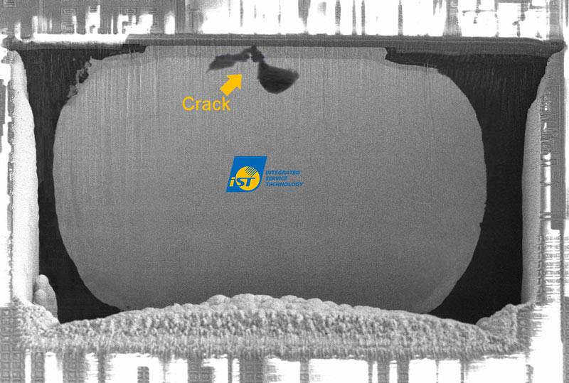
Figure 7: A clear solder ball defects shown
The silicon substrate removal from the die’s backside can be used not only for identifying solder ball defects by advanced packaging but also for locating broken circuit (Figure 8) or modifying circuit in ICs from their backside by advanced process (see How do we do backside FIB circuit editing for advanced process IC?).
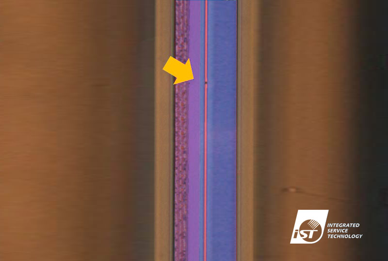
Figure 8: Broken circuit found by the “die’s backside” approach
This article is aimed to share our experiences with honorable clients like you. In case you want to know more details, please call Mr. Sam Wu at +886-3-579-9909 Ext. 6738 or email: web_decap@istgroup.com