Issued Date:2020/4/16SMT DOE Tests
Issued By:iST
Are you short of suppliers to conduct the SMT tests in small but various batches in R&D phase?SMT DOE Tests
Are you suffering poor estimation of products’ life span due to poor SMT quality when validating advanced packaging and IC chip service life and performance?
Are you troubled by SMT sample preparation for testing quality of ICs on-board due to the increasingly smaller size of ICs?
Addressing the growth of IoT, AI, and auto-pilot, it is now trending in the direction of fast transmission and processing of huge amount of data. When High Performance Computing (HPC) is getting critical in the R&D of process technology and the complexity of design and packaging is ever rising, advanced packaging is poised to be the key factor in extending the validity of Moore’s Law.
The greatest technical challenge faced by advanced packaging technology lies in integrating hetero materials of IC chips. This may come in form of warpage due to complex stacking. Another common challenge in board level reliability is subject to the connection of very fine lines and spaces by SMT(Surface Mount Technique).SMT DOE Tests
With more than 25 years of experience in the semiconductor verification industry, iST has been approached by customers for SMT services in the NRE (Non-Recurring Engineering) and DOE (Design of Experiment) stage for several years. These small-and-various-batch requirements are usually aimed at material selection and process parameter tuning before mass production.
Being an engineer of the semiconductor industry, you must have been troubled by a lack of in-house SMT production capacity to support R&D goods required in small but various batches in NRE and DOE stage while IC design engineers may have also been denied by large OSATs (Outsourced Semiconductor Assembly and Test Providers) for the same services.
iST knows your needs. Our SMT service unit is not only assisting you in preparing tailor-made SMT DOE test samples for quality and reliability verification but also in conducting engineering DOEs and optimizing the combination parameters to deal with the SMT issues found during the R&D process.
Which role is Surface Mounting Technology (SMT) playing during product R&D? The quality of IC mounted on simulation PCBs shall have a direct impact on the precision of estimation over product service life. Key factors of quality are solder paste features, mounting conditions (including demolding distance, demolding time, and printing speed), components inserting accuracy, and steel plate selection, as shown in figure 1.

This iST Tech Classroom is to share with you three common SMT cases required by customers.
Case 1: Mount and Demount Balls on Substrate Manually
Materials of solder balls are critical to product quality. Any material quality issues found at mass production stage are most likely too late to recover.
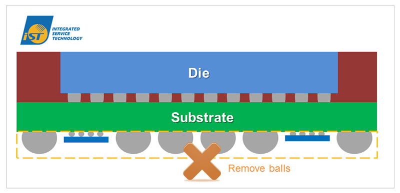
iST’s reliability verification lab is working with customers to identify the optimum formula of solder balls at the initial stage of product design. The ball mounting comes in two application types:- Verification over the ball’s solder reliability: mount balls to be verified on substrates with special jigs.
- Verification over the ball’s bracing status: component size expands with advances in packaging technology which, in turn, results in warpage caused by size and short circuit caused by soldering error due to the weight of the component body. The iST’s reliability verification lab is raising the bracing strength and preventing soldering failure caused short circuits by mounting balls with copper cores on the substrate (Figure 2). The solder balls may come in different alloys (e.g. SAC305, SAC405 alloys ) and cores (e.g. copper core). You may identify appropriate balls to raise a product’s verification success rate by mounting balls on the substrate for DOE.

Figure 2: iST’s tin ball mounting process
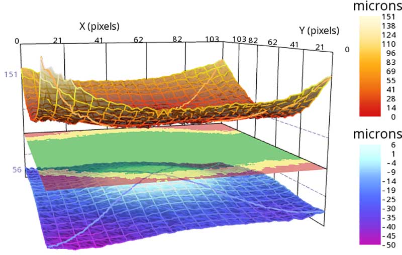
In term of ball demounting process, addressing varying packaging approaches, iST is offering a customized process to assist customers in their demounting operation. In case the sample has silicon attached on its backside, iST shall take the required pre-demounting operation for successful warpage measurement simulation (Shadow Moiré) later.
Figure 3: iST’s ball demounting process
Case 2: Recommend Parameters for SMT Solder Joint
Complex hetero material integration and stacking tends to result in over-warpage. The iST reliability verification lab is approached by many IC design houses, fabs, and OSATs to simulate warpage data. They are aimed to tune the design of solder paste stencil and reflow temperature to reduce non-wetting and solder bridged caused by warpage. iST has solved the solder joint problem caused by PCB or IC warpage for some customers with this method successfully.
Case 3: POP (Package on Package) Case for Board Mounting Alignment
This is the case of sandwiching two PCBs (upper and lower) with solder pastes in between to mount the component (Figure 4). This may result in PCBs’ bumping or bending and the need to be tackled by jig alignment.
The making of jigs has to take the aperture size and thickness of solder paste stencil, as well as the exact positioning of the upper and lower PCBs into account. iST is here to assist you in making jigs, board mounting, and soldering quality validation by X-ray in its failure analysis lab later.

Figure 5: iST provides custom jigs for alignment
This article is aimed to share what we have learnt on this with honorable clients like you. iST is offering more SMT capacity to not only prepare SMT DOE Tests samples required by reliability tests, but also rendering services for production in small but various batches. Should you have any inquiries, just ring Mr. Chang at +886-3-579-9909 EXT 6429 or email us at WEB_SMT@istgroup.com。


