Issued Date: 2018/8/8
Issued By: iST
How do you effectively reduce RDS(on) (on-state-impedance) when the MOSFET power semiconductor chip is red hot?
MOSFET has been playing the role of “switch socket” for a long time in the electronics world. Featuring a high switching speed, low input impedance and low power consumption, it not only withstands high currents but also improves circuit conversion efficiency, and these factors combined made it a critical power component.
Pursuing high-efficiency power conversion and low power consumption, manufacturers found a shortcut: reducing RDS(on).
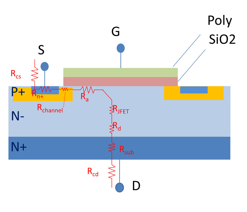
RDS(on) is composed of several impedances: source contact impedance Rcs, N+ internal impedance Rn+, channel impedance Rchannel, accumulation zone impedance Ra, JFET region impedance RJFET, drift region impedance Rd, substrate impedance Rsub, drain contact impedance Rcd, and sum of package impedance Rpack.
How to effectively reduce RDS(on) without spending too much cost on R&D? Try these 3 recommendations by iST:
I. Begin with Si process and design
This method has been widely adopted in the past 10 years. Recently, we have observed several MOSFETs with low RDS(on) from leading brands, including CoolMOS by Infineon based on the multi-layer epitaxial stack technology, the MDMesh by STMicroelectronics, DTMOS by Toshiba, and SuperMOS by Fairchild, which employ deep trench refill technology. OnSemi used this, along with a Liner oxide design, in its UltiMOS to reduce RDS(on) via a super junction with higher N-type Epi concentration without loss of depth in the depletion region. The CoolMOS by Infineon has been remarkably well accepted by the industry since its launch in 1998, and more than 1.6 billion pieces of it have been sold in last three years(Note1).
II. Improve its package
MOSFET RDS(on) can be lowered in the packaging process: reduce wire resistance with a clip to expand the current path (to replace gold wires) via clip bond and diffusion solder as well as lower impedance between metals with intermetallic compound formed between heterogeneous metals layers.
III. Try thinning the wafer
As mentioned earlier, RDS(on) is determined by the sum of a series of resistance sums. Part of it is subject to Rsub which, in turn, is related to the doping concentration and the thickness of the wafer itself. That is, thinning substrate may lower RDS(on). The “wafer thinning” technique has been adopted by the industry in recent years to make wafers thinned.
For thinning the substrate in item 3, the new “MOSFET wafer backend process integrated service” launched recently by iST has been received some customers’ requests for wafer thinning. To make wafers of very precise, very thin thickness is quite challenging technology. First of all, it is quite difficult that thinning wafers to reach a certain thickness, as the edge of the wafer tend to warp when wafer being thinned. Warped wafers may result in difficulties in the subsequent processes as they are fragile during shipment or during manual handling (when auto-handling fails due to warpage). iST employs the Taiko technique to overcome this issue. By leaving a Taiko ring on wafer edge, similar to drum ring, leaving edge of wafer with partial precise grinding on wafer center, the wafer may come out without warpage. The process of thinning wafers to 50um as been verified and is now in mass production for multiple customers with line yields up to 99.5%. The 37.5um and 25um Taiko technology is now in engineering verification.
Regarding “precise” thinning, iST has been approached by customers for wafer thinning to 100um and 50um for lower RDS(on). By applying simultaneous etching technology, iST is able to obtain good wafer uniformity with total thickness variation (TTV) well controlled within 3um. We found that only thinning wafers from 100um to 50um can reduce RDS(on) 19% (Note2)in same testing condition and same device design without any design changes nor any modifications to processes in the foundry or backend packaging plant.
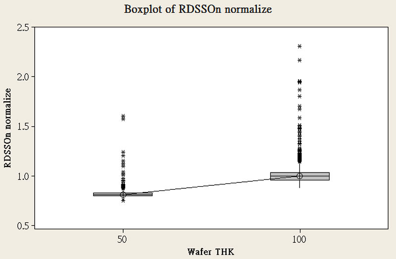
Caption: By thinning the wafer from 100um to 50um with our techniques, iST can help customers
to lower power MOSFET RDS(on) around 19%.iST is continuing to advance its wafer thinning techniques. The 15um version is ready now. As illustrated below, the wafer is as thin as an organdy, actually almost transparent, and emits red light when illuminated with a white light source. iST is more than happy to co-work with customers to offer power MOSFET backend engineering service to fine-tune process for lower RDS(on) .
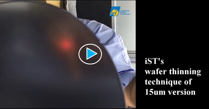
Click this link or the image above to view the 15 um wafer thinning video
Note 1:Refer to a report of Digitimes: 滿足MOSFET需求 英飛凌CoolMOS系列性價俱佳,賴品如,2018/6/27,2018/7/24 visited.
Note 2: This illustrates the outcome of chip probe (CP), comparisons are made after normalization.
It’s our pleasure to share iST’s techniques with you. Should you have any requirements for RDS(on) reduction or wafer thinning, please call Mr. Yu(Stan) at +886-3-579-9909 Ext. 5888 or send an email to web_sp@istgroup.com.