Issued Date: 2016/7/28
Issued By: iST
IC Electrical test failed on IC after packaging, Bad chip design or IC packaging defect – which one is to blame?
PCBA test defect, Poor chip design, improper packaging process, or surface mounting/soldering error – how to determine the real causes?
You may have encountered all these problems. To identify their causes, you have to face the same challenge: The tool you can use for testing must be non-destructive, e.g. an X-ray.
Most X-ray machines suffer limited resolution and low magnification which hampers identifying tiny defect and wastes a lot of time fact-finding and correction.
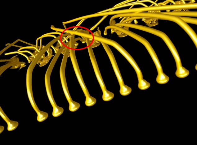
Addressing this, iST has upgraded its equipment stock with a ZEISS Xradia 520 Versa, a cutting-edge High Resolution 3D X-Ray Microscope, for industry leading resolution, highest magnification ratio, and 360 degree panoramic imaging.
More important than easily identifying outliers, the upgraded machine can now test more diversified samples in size and type. Scores of samples, including normal IC and 3D IC, MEMS, as well as PCBs, PCBAs, and finished products can be non-destructively tested at iST as long as they feature a footprint up to 30cm and weight up to 15 kilograms.
Case 1
Case 2
Case 3
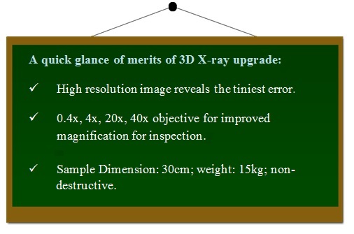
Passive component failure. Thermal EMMI testing on samples indicates leakage first while a 3D X-Ray test finds foreign metal matter left inside.
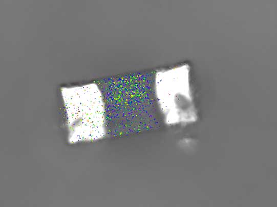
Image by thermal EMMI
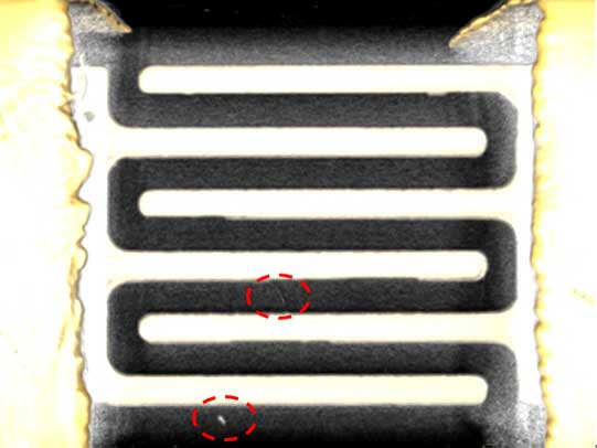
Image of foreign metals by 3D X-Ray
To further learn about these abnormalities, iST may provide dye and pry test after 3D X-Ray for comprehensive diagnosis:
PFA (physical failure analysis): pin point error position with 3D X-Ray first and verify with slicing.
CRE (component reliability): cracks in limited area found by 3D X-Ray, run dye and pry test to determine overall cracks on solder joints.
To learn about the applicability of employing 3D X-Rays in testing errors found in your products, please refer to application cases outlined below:
- Inspection of flaws in IC packaging: inspections of wire bonding, electrical test error (open/short), molding compound cracks or bubbles, and epoxy voids, etc.
- Flaws in the PCB and carrier board process: such as circuit alignment or bridge and open circuit, quality inspection of plated via process, multi-layer PCB layout analysis.
- Electronic product flaws, including open circuits, short circuits, and disconnection errors.
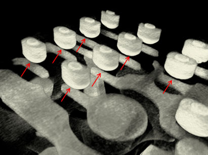
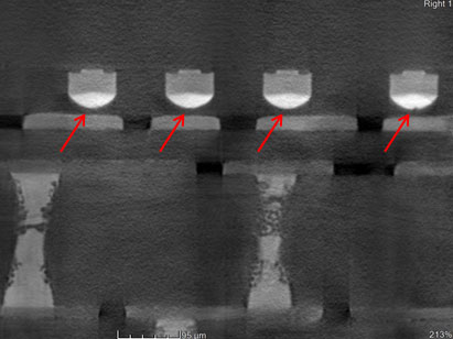
- Solder joint integrity inspection of BGA and flip chip packages, including solder ball deformation, cracks, non-wetting, cold joint, short, and voids.
- Crack inspection of high-density plastics or cavity inspection of metals.
- Active and passive component inspection and analysis.
- Material structure inspection and analysis & dimension measurement.
We are more than glad to share our inspection and test experiences with you. In case of any needs for abnormality inspection or determination suffered by your products or further information on 3D X-Ray, please call Miss Chen at 03-579-9909 Ext. 6071 or Mr. Chang at Ext. 6074 or send email to web_nde@istgroup.com.