Issued Date: 2014/10/7
Issued By: iST
Problems occur at high current after pilot run of IC production?
IC internal short-circuit unsolved when end customer ready for mass production?
Unable to verify whether the cause of customer rejection is in the die or in the package?
Identified defects cannot be further clarified as in which layer due to 3D packaging?
 You may have encountered some of the above problems, more or less. iST has heard your needs and introduced Thermal EMMI (InSb) for detecting defects without de-capsulation of IC., including a low-resistance (<10ohm) short-circuit detection function that enables quick positioning of defect coordinates by detecting distribution of thermal radiation when IC is powered on.
Furthermore, for 3D packaged products, defects were identified in the past by cutting lines layer by layer, which consumes time and effort. Our newly acquired Thermal EMMI helps you rapidly identify the defect is in which layer of the die by estimating the depth of defect in the 3D packaging (the z-axis direction) via time difference of thermal radiation transmission. Naturally, the same technique can be used for detecting defects in TFT LCD Panels as well as for failure analyses of PCBs/PCBAs.
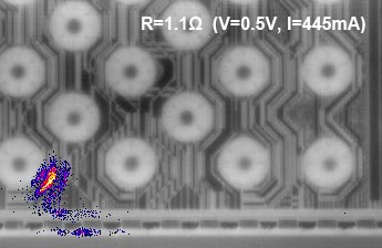
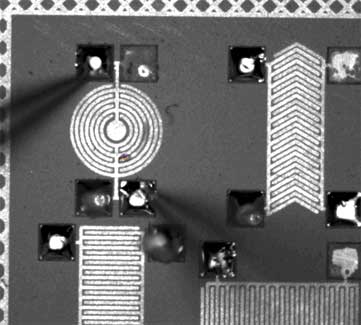
Here are several typical Thermal EMMI examples. In low magnitude, IC Top Marking (Fig.1) can be seen clearly. In short-circuit failure samples with extremely low resistance, not only the light spots are clearly seen under the Thermal EMMI, the relative coordinates of the spot are also shown (Fig.2).
Fig.1
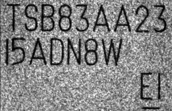
Fig.2
The following Fig.3 shows the bright spot without de-capsulation, easily revealing whether the problem lies in the die or in the packaging. As for PCB short-circuits which have rather large volumes, defects can all be identified (Fig.4).
Fig.3
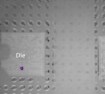
Fig.4
In general, Thermal EMMI (InSb) of iST is capable of detecting the following defects for you:
- Short-circuit of IC bonding wire and/or IC internal circuit
- Current leakage of dielectric layer (Oxide)
- Current leakage in transistors and diodes
- Metal circuit defects and short-circuits of TFT LCD Panel and PCB/PCBA
- ESD Latch-up
- Estimation of depth of defect in 3D package (stacked die)
We believe the energy of this newly acquired device will help you identify defects more precisely and more effectively in dealing with the time specific development/mass production/customer rejection. For any relevant need, do not hesitate to contact us at +886-3-579-9909 ext. 6767, Mr. Chen (Teron) │Email: web_ise@istgroup.com