Issued Date:2024/7/16 TEM EDS light elements
Issued By:iST

When it comes to light elements like carbon, nitrogen, and oxygen, does TEM/EDS compositional analysis become inaccurate? It turns out that low-energy X-ray absorption is the culprit. Understanding and overcoming this issue is crucial for improving component reliability and the accuracy of compositional analysis. This article will delve into this phenomenon and uncover the mystery behind the distortion of light element analysis in TEM/EDS.
TEM EDS light elements
As semiconductor technology continues to advance, the importance of nanoscale compositional analysis in the development of new processes is becoming increasingly prominent. Using TEM/EDS techniques, researchers can deeply identify compositional information in nanoscale regions. However, during TEM/EDS compositional analysis, especially when it involves light elements like carbon, nitrogen, and oxygen, the effect of low-energy X-ray absorption remains significant, and the amount absorbed varies with the thickness of the sample.
Coincidentally, compounds of these light elements are commonly used materials in semiconductor device manufacturing. Therefore, when performing compositional analysis of semiconductor devices using TEM/EDS, the presence of elements like carbon, nitrogen, and oxygen can increase inaccuracies. Accuracy can be improved by some special calibration techniques. This article introduces absorption effect of light elements only, calibration techniques will be discussed in the next issue.
TEM EDS light elements
TEM EDS light elements
I. Introduction of EDS of light elements
EDS compositional analyzers can be mounted on both TEM and SEM electron microscopes; this article focuses on compositional analysis techniques specific to TEM/EDS. Regarding the differences between TEM/EDS and SEM/EDS, we briefly introduced them in the previous article (read more: Intelligent Interpretation of True or False Signals in EM/EDS Analysis).
Absorption effect is very serious in SEM/EDS analysis, especially when light elements are involved. ZAF(Z/atomic number;A/absorption;F/fluorescence)calculation has to be applied for quantitative analysis in SEM/EDS. Specimens of thin foils are used in TEM analysis. Thus, absorption effect is considered to be neglected in TEM/EDS analysis by many people. This is true for some material systems, such as metals.
However, we have found that absorptions of X-Rays of low energy emitted from atoms of carbon, nitrogen, or oxygen, which are commonly used in manufacturing semiconductor devices, are still significantly from hundreds of TEM/EDS cases. Meanwhile, the effect of absorption varies with the specimen thickness. Inaccuracy of TEM/EDS quantitative analysis will increase when one or more light elements are involved.
Two TEM/EDS spectra of nitride and oxide are shown Figure 1. The EDS spectrum in Figure 1(a) is from an interfacial region of TiN/SiO2, indicated by the orange circle in the inserted TEM image. This is a local part of a basic structure of semiconductor devices. The EDS spectrum in Figure 1(b) is from a GaN layer indicated by the orange circle in the inserted TEM image. All SiO2, TiN, and GaN are stoichiometric compounds. The ratio of atoms for oxygen to silicon is 2: 1 in silicon dioxide, for nitrogen to titanium is 1: 1 in TiN, and for nitrogen to gallium is 1: 1 in GaN. Theoretically, the peak intensity of an element is proportional to its concentration in the material analyzed. Thus, the peak intensity of oxygen should be twice as high as that of silicon, and the peak intensity of nitrogen should be equal to that of titanium or gallium. But actually, peak intensity of N and O is much lower that of Si, or Ti, or Ga, as shown in Figure 1. There are two mechanisms involved to result in the final result, and will be discussed following.
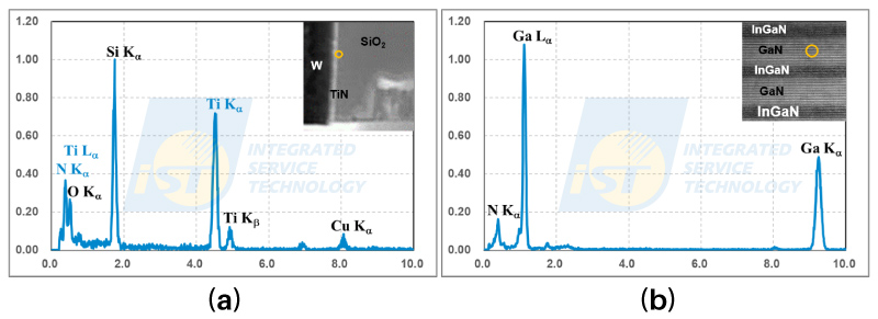
Figure 1: TEM/EDS spectra of nitride and oxide. (a) SiO2 + TiN;(b) GaN.
(Source: iST)2. Sensitivity Curve of EDS Detector
Firstly, it is a natural characteristic of EDS detectors. The sensitivity of the EDS detector for X-Rays through the spectrum is not unique. The sensitivity curve of the EDS detector is displayed in Figure 2(a). The sensitivity in the range of 3.0 ~ 19.0 KeV is one, and drops quickly in the low energy region, while drops slowly in the region higher than 19.0 KeV. The mechanism of reducing sensitivity is different in these two ends. The probability of passing through the crystal directly without producing electron-hole pairs in the crystal increases with energy of X-Rays beyond 19.0 KeV, and it leads to reduce the sensitivity. In the low energy region, the sensitivity of the EDS detector decreases due to the attenuation of some detector components. Three components, window/gold electrode/dead layer depicted in Figure 2(c), in front of the detector crystal attenuate X-Rays of low energy. Lower energy X-Ray is, more is attenuated. X-Rays with energy less than a certain value are complicatedly blocked to enter the crystal.
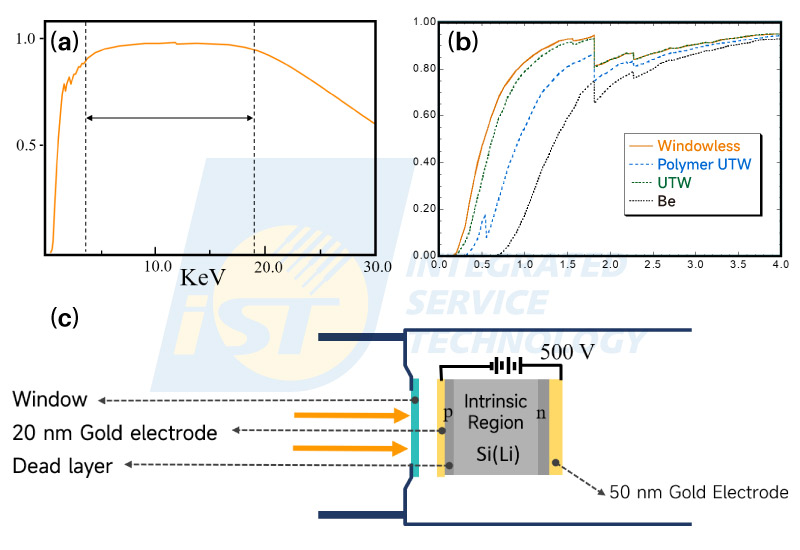
Figure 2: EDS detector. (a) Sensitivity curve of EDS detector, (b) Magnified sensitivity curve of EDS detector low energy region. (c) Simplified Cross-Section Diagram of the Detector Structure
(Source: iST)The window is the main part to attenuate X-Rays among these three. Beryllium windows of 7 ~ 12 micrometer were used first. This kind of EDS detectors are very durable, but not able to detect X-Rays of oxygen and elements of smaller atomic number. By using polymer ultra-thin-windows in place of Be windows, carbon can be detected by EDS detectors. Both performance and efficacy of EDS detectors have been improved a lot since 2010. Meanwhile, Silicon Drift Detectors (SDD), which are gradually replacing Lithium-drifted silicon detectors (Si(Li)D), coupled with windowless make the sensitivity of oxygen be increased more than 2.5 times[3]. Even though, the trend of quick drop in low energy region remains same.
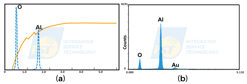
Figure 3: Schematic diagram of EDS spectrum (a) and a real EDS spectrum (b) of Al2O3.
(Source: iST)The final EDS spectrum is a convolution of X-Rays entering the detector with the sensitivity curve of the detector. The basic concept of convolution is illustrated in Figure 3. Energy peaks of blue dashed lines represent idea intensity of O and Al when Al2O3 is stroke by electron beams, the peak intensity of O is one and half times of that of Al. The orange curve is the sensitivity curve of the EDS detector. The real EDS spectrum in Figure 3(b) is the final result of convolution of them. The peak intensity of O is much less than that of Al. Therefore, we have to divide the peak intensity or the integrated intensity of elements by their corresponding sensitivity factors to calculate their real concentration. A litter change in oxygen intensity will result in significant fluctuations, and increases the inaccuracy in the final result.
3. Absorption of X-Rays
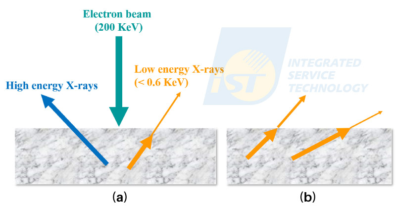
Figure 4: Schematic diagram of escaping of X-Rays of high energy (blue arrow) and low energy (orange arrow) from a thin foil specimen. (a) Escaping rate of X-Rays of high energy and low energy, (b) escaping rate of low energy X-Rays travelling along different path.
(Source: iST)The second effect reducing intensity of O or N is absorption. X-Rays generated in the specimen have to escape from the specimen, then can be detected by the EDS detector. The escaping rate of X-Rays decreases with decreasing energy and the length of travelling paths. X-Rays which fail to go out of the specimen are called to be absorbed by the specimen. The red arrow represents high energy (> 1 KeV) X-Rays, and the pink arrow represents low energy (< 0.6 KeV) X-Rays. All high energy X-Rays escape from the specimen, while only parts of low energy X-Rays escape from the specimen. For TEM specimens, the effect of absorption becomes significant gradually for energy of X-Rays is lower than 0.6 KeV, and increases with increasing specimen thickness. The travelling paths of X-Ray are random. Those paths with small angles to the specimen surface are longer than those with large angles, as illustrated in Figure 4(b). The absorption rate increases with the length of travelling path. That’s why high angle EDS detectors have better sensitivity for light elements.
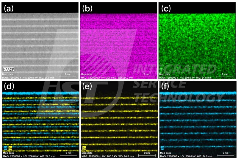
Figure 5: STEM/EDS Analysis of InGaN/AlGaN /GaN multi-quantum well. (a) STEM HAADF image, (b)Ga map, (c)N map, (d)Al + In map, (e)In map, (f)Al map.
(Source: iST)The thickness of TEM specimens prepared by FIB are usually considered to be constant compared with those wedge-shaped TEM specimens prepared by mechanical grinding and polishing. However, the thickness of TEM specimens prepared by FIB increases downward slowly due to the shielding effect. This change in specimen thickness affects nothing for TEM BF images, and not obviously for HRTEM images, but significant for absorption of low energy X-Rays. A set of STEM/EDS spectrum image of InGaN/AlGaN/GaN multi quantum wells are shown in Figure 5. The brightness of elemental maps of Ga, Al, and In are homogenous through maps, this means that their X-Ray intensity is same in these analyzed area. On the contrary, the brightness of the N map is decreasing downward gradually. This N map indicates that nitrogen X-Rays intensity detected decreases downward. A set of EDS line profiles, shown in Figure 6, extracted from this spectrum image display the decrease in N more precisely. The ratio of N to Ga kept same during MOCVD process was confirmed by the sample supplier [4]. Thus, the decrease in nitrogen concentration in Figure 6 is induced by absorption effect. Only parts of X-Rays of nitrogen, 0.392 KeV, were absorbed in TEM specimen of thicker and thicker, and it cause the decline in its concentration.
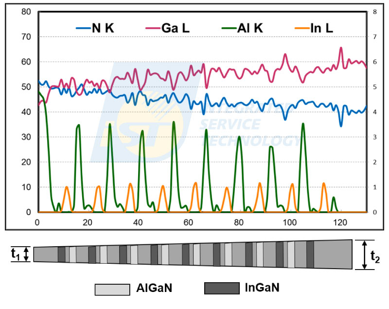
Figure 6: EDS line profiles of InGaN/AlGaN/GaN multi-quantum well(upper) and schematic diagram of TEM specimen (lower).
(Source: iST)In order to confirm that the decrease in N concentration in Figure 6 is caused by absorption effect with increasing specimen thickness, EDS line profiles as shown in Figure 7 are extracted along paths of 130 nm horizontally (equal thickness direction). The ratio of N/Ga is a little different at these two positions, anyway the ratio of N/Ga keeps for both horizontal positions. These data prove that absorption of low energy X-Rays can be affected by the variation of TEM thickness.
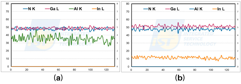
Figure 7: EDS line profiles of InGaN/AlGaN/GaN multi-quantum well along paths of equal thickness. (Source: iST)
TEM/EDS which is able to characterize chemical information of Nano-scale regions is the main analytical technique for composition analysis in semiconductor devices. It offers important chemical data for developing new semiconductor processes. Types of TEM/EDS analyses can be divided into qualitative analyses and quantitative analyses. The former characterizes what kinds of elements exist in the analyzed area and their approximate relative content, which is currently the most common task in EDS analysis. The later analyzes the elemental concentration to a certain of accuracy to identify what a compound is, or what an alloy is. The accuracy of TEM/EDS can reach 2% if enough intensity, such as more than 2000 counts, is collected. However, when the analyzed region is consisted of light elements, such as C, N, O, the accuracy may be decayed to 5 ~ 10 % due to the EDS sensitivity and absorption effect.
The accuracy can be improved to be better than 5%, or even 2%, if some reference materials of stoichiometric composition, which behaves as a standard for calibration, are available around. The method of calibration using one or two reference materials will be discussed in next iST material classroom
iST’s Material Analysis Laboratory has extensive experience and successful cases in the semiconductor process and advanced packaging fields. In this article, we share this knowledge with our long-time supporters. If you have related needs or would like to further understand this knowledge, please feel free to contact marketing_tw@istgroup.com.
References::
[1] David B. Williams and C. Barry Carter, in Transmission Electron Microscopy, Microscopy, part IV, Plenum Press, New York (2007). ISBN: 0-471-122440-0
[2] R. E. Lee, Scanning Electron Microscopy and X-Ray Microanalysis, pp. 329-406, PTR Prentice Hall, Englewood Cliffs, New Jersey (1993). ISBN: 0-13-8137590-5
[3] FEI DM (2012)
[4] T. U. Wang, W. C. Lai, S. Y. Sie, S. P. Chang, C. H. Kuo, J. K. Sheu J. S. Bow, “AlGaN-based Deep Ultraviolet Light-emitting Diodes with Thermally Oxidized AlxGa2-xO3 Sidewall,” J. ACS Omega, (2022) .