Issued Date:2024/6/25 TEM EDS analysis
Issued By:iST

As the semiconductor manufacturing process approaches its limits, materials analysis has become crucial for overcoming bottlenecks. In the industry, electron microscopes coupled with X-ray energy dispersive spectroscopy (EDS) are often used to analyze micro and nanoscale materials.
However, the energy resolution of EDS is relatively low, leading to two major issues: peak overlap and false signals. How should one interpret EDS spectra to accurately determine the material composition?
TEM EDS analysis
As semiconductor manufacturing approaches its physical limits, major companies worldwide are continuously focusing on materials to overcome research and development bottlenecks. Materials analysis is crucial for improving semiconductor defects and enhancing manufacturing yield. Today, engineers often use electron microscopes equipped with X-ray Energy Dispersive Spectroscopy (EDS) to analyze micro and nanoscale materials. This tool enables to identify microstructure and the composition of micro and nanoscale regions simultaneously. (Read more: How to Identify & Analyze Ga2O3)。
Due to the low energy resolution of EDS, energy peak overlap frequently occurs in EDS spectra. Additionally, the scattering of the electron beam can generate false signals known as ” spurious X-rays.” These two issues are significant sources of error in material composition analysis. In this article, we will guide readers on how to intelligently interpret the authenticity of copper signals in EDS spectra, distinguish peak overlaps, and analyze the correct composition distribution map.
TEM EDS analysis
TEM EDS analysis
1.Introduction of EM/EDS Analysis
Electron microscopes (EMs) mentioned in this article, including scanning electron microscopes (SEM) and transmission electron microscopes (TEM), and we will primarily focus on the latter. The energy resolution of EDS is very poor compared with other composition techniques used in electron microscopes, as shown in table 1. However, the simplicity of operation and data process and low price make EDS most popular in the field of material analysis, especially in semiconductor industry.
Table1: Comparison of characteristics of spectrometers in electron microscopes.
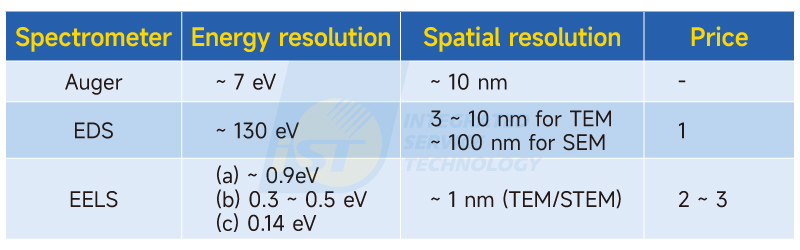
(Source:iST)
The main difference of EDS analysis in SEM and TEM is illustrated by Figure 1. Specimens of buck type are used in SEM. The volume of X-Rays generation is large due to the effect of beam broadening[1, 2], this results in the poor spatial resolution in SEM/EDS analysis. Usually, the operation voltage of SEM can be adjusted from 5 to 30 KV to check the variation of microstructure in depth. While TEM/EDS analysis is performed in a fixed operation voltage used routinely. We usually operate TEM/EDS analysis at 200 KV to analyze inorganic solid materials.
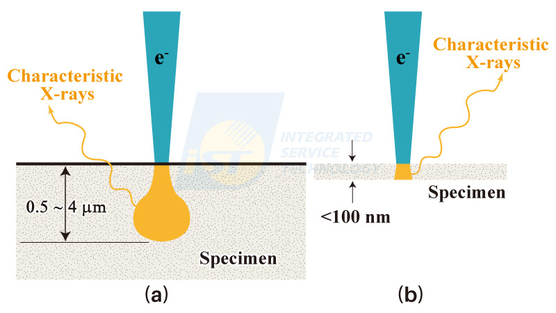
Figure 1:Schematical diagram shows the relationship between specimen morphology and volume of X-Rays generated. (a) a SEM specimen of smooth surface, (b) a TEM specimen. (Source:iST)
2. How to Interpret Spurious X-Rays in EDS Spectra
Overlap occurs in EDS spectra from time to time due to its poor energy resolution, 130 eV. It will be one of topics of this article to interpretate those overlapped energy peaks. The second type of artificial signals in EDS spectra is spurious X-Rays which are induced by scattered electrons.
When the surfaces of SEM samples are rough, some X-Rays are generated from regions away from the incident beam by scattered electrons, as indicated in Figure 2(a). There will be no problem if these spurious X-Rays are generated from regions of composition same with the analyzed region. It will make puzzles if these spurious X-Rays are generated from regions of composition different from the analyzed region. Spurious X-Rays become complicate when they are induced on a rough surface of a SEM sample. Unless in cases of fracture surfaces, SEM specimens are ground and polished to be smooth surfaces when EDS analyses are required. So, the possibility of generating spurious X-Rays is removed.
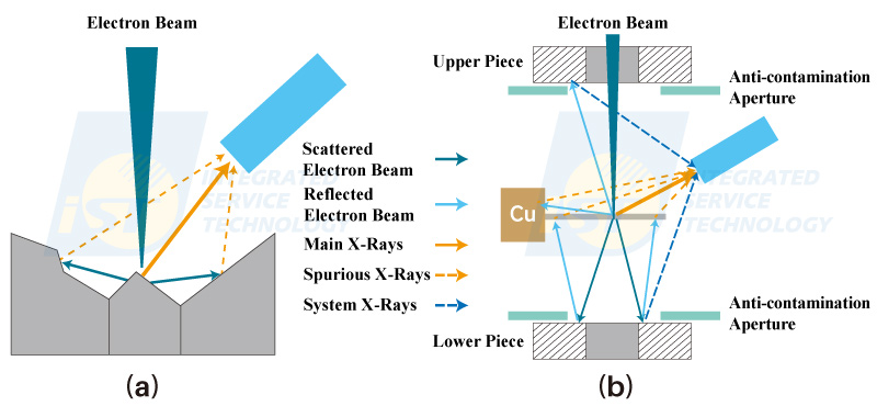
Figure 2: Schematical diagram shows how spurious X-rays are generated. (a) a SEM specimen of rough surface, (b) a TEM specimen in working chamber. (Source:iST)
This article will discuss spurious X-Rays in TEM/EDS only. From Figure 2(b), we figure out that spurious X-Rays result from Cu rings, which are widely used to support TEM specimens, and objective lenses. When spurious X-Rays are generated from pole pieces (objective lenses), they are called system X-Rays[3],, since pole pieces are parts of the TEM system. System X-Rays are blocked to enter the EDS detector by adding a collimator in front of the EDS detector, because they travel along trajectories of high angles to go into the EDS detector, as illustrated in Figure 2(b). Following, we are going to focus on spurious X-Rays from Cu rings. Cu rings and Cu grids are widely used to support TEM specimens. Thus, Cu peaks are observed in many TEM/EDS analyses sometimes, as shown in EDS spectra in Figure 3. Spurious X-Rays will become Ni X-Rays when Ni rings instead of Cu rings are used to support TEM specimens.
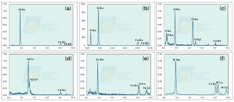
Figure 3: Normalized EDS spectra. (a) Si, (b) SiO2, (c)SiO2 + TiN, (d)Ag, (e)Ag, (f)W. The peak intensity of Cu Kα increases with the average atomic number of the analyzed material. (Source:iST)
Cu signals in normalized EDS spectra in Figure 3 display two characteristics.
(1) Only Cu Kα peaks but not Cu Lα peaks are observed in these EDS spectra.
(2) The peak intensity of Cu Kα increases with the atomic number of the analyzed material. A trend chart, Figure 4, is drawn by collecting data of TEM/EDS of specimens supported by Cu rings.
The horizontal axis of the Figure 4 is atomic number, and the vertical axis of the Figure 4 is the ratio of the peak intensity of Cu Kα to the peak intensity of X Xα, where X stands for the major element analyzed, such as Si Kα or Ta Mα. Data in Figure 4 clearly point out that Cu Kα peaks are observed in EDS spectra even no Cu in these analyzed specimens, and their intensity increase nonlinear with the atomic number of analyzed materials. X-Rays of Cu Lα were generated simultaneously but were too weak to escape from Cu rings. A TEM/EDS spectrum from a pure Cu region is shown in Figure 5(a), the peak of Cu Lα is higher than that of Cu Kα. Similarly, a TEM/EDS spectrum from a pure Ni region was acquired and shown in Figure 5(b), the peak of Ni Lα is as high as that of Ni Kα.
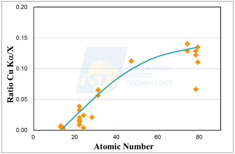
Figure 4: The trend plot of the ratio of the intensity of Cu Kαto the intensity of X Xα of element X with the atomic number. (Source:iST)
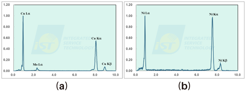
Figure 5: Normalized EDS spectra. (a)Cu, (b)Ni. (Source:iST)
A set of rules are drawn by summing up data in Figure 3 to Figure 5. We thus can judge those Cu signals in EDS spectra of thin films to be spurious X-Rays rather than Cu elements in thin films by these rules. So, we know that those sputtering targets were contaminated by Cu. It is the responsibility of engineers of materials analysis to give their customers correct information of materials analysis. Correct interpretation of material analysis data can help engineers in departments of R&D and departments of process to save lots of time and resources in yield enhancement.
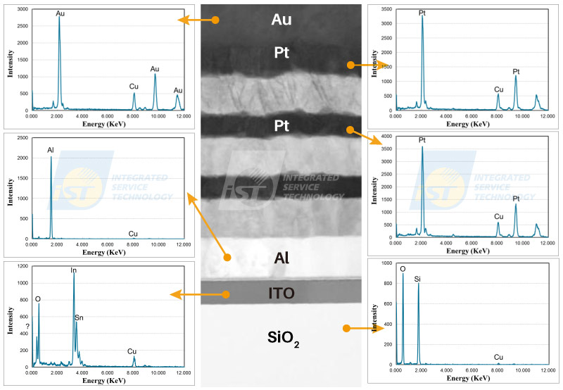
Figure 6: STEM/EDS Analysis of a multi-layer thin film material. Only Cu Kα but not Cu Lα is shown in each EDS spectrum. Intensity of Cu Kα increases with the average atomic number of the thin film. (Source:iST)
3. Distinguishing Overlapped Energy Peaks and Extracting Composition Distribution
As mentioned early, the most common overlap in semiconductor devices is Si Kα(1.740 KeV)/ Ta Mα(1.709 KeV)/ W Mα(1.774 KeV), illustrated in Figure 7. Three normalized EDS spectra are included in Figure 7, they are Si, Ta, and W respectively. The energy peak of Si Kα/ Ta Mα/ W Mα is indistinguishable when they put together. In the front end process of semiconductor devices, an important structure is consisted of W plug/silicide/Si substrate, as shown in Figure 8(a). An EDS line profile acquired along the path marked in Figure 8(a) will display data shown in Figure 8(b). Raw EDS data are used to process this set of EDS line profiles, and a orange curve stands for Si concentration runs from W plug, through silicide, to Si substrate. This is obviously incorrect in W plug. A set of new EDS line profiles after adequate process is shown in Figure 8(b), there Si signals are no longer in the W plug.
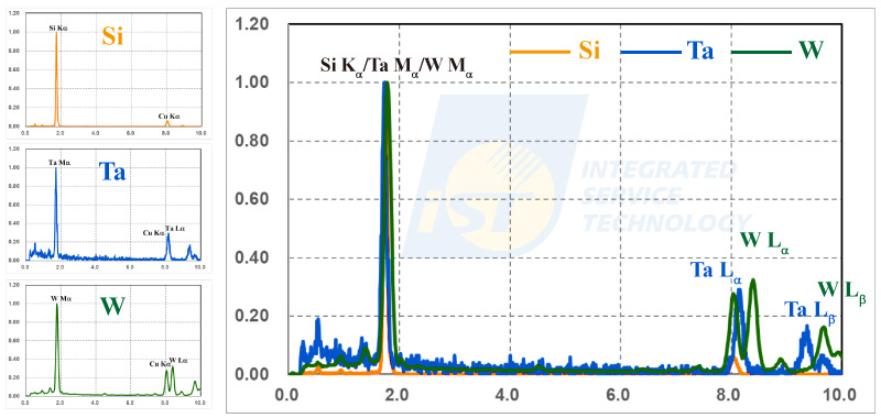
Figure 7: Normalized EDS spectra of CoSi2, Ta, and W. Three EDS spectra are put vertical individually at left side and combined into one at right side. (Source:iST)
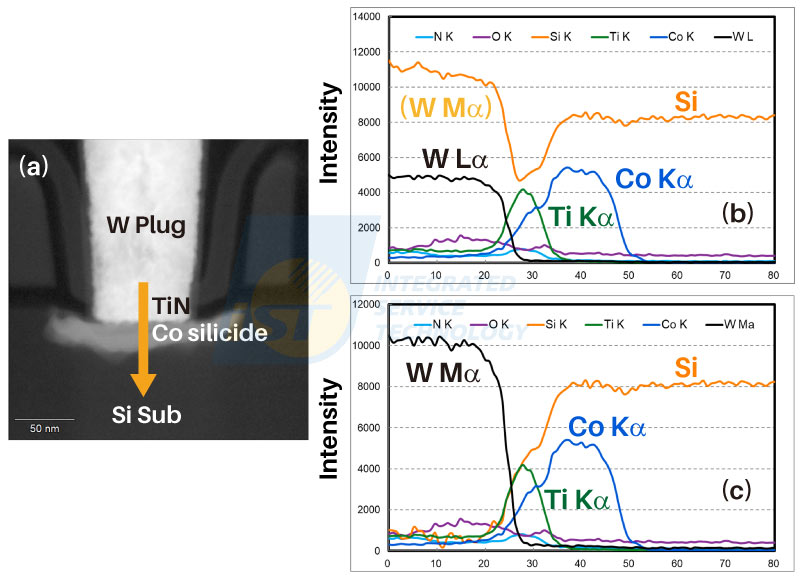
Figure 8: STEM/EDS line profiles of a semiconductor device. (a) STEM HAADF image, (b) raw EDS line profiles, (c) processed EDS line profiles. (Source:iST)
Currently, all famous EDS factories have developed powerful software which are able to process EDS data as well as control the acquiring EDS data of various model. All these software have the capability of processing overlapped energy peaks. Objects of these data operations are spectrum images rather than individual EDS spectrum or EDS line profiles. Acquired raw EDS data have to be processed firstly, and a set of processed spectrum image is generated, then correct EDS spectra, especially correct EDS line profiles can be extracted from this processed spectrum image. If EDS line profiles are extracted from raw EDS spectrum images or acquired directly, results will be those shown in Figure 8(b). The overlap of W Mα and Si Kα can be separated by using data of W Lα and the intensity ratio of W Mα and W Lα, then correct EDS line profiles can be obtained. Corrected EDS line profiles in Figure 8(c) were obtained by using data in Figure 8(b). The advantage of performing EDS line profile analysis directly is to save lots of acquisition time in TEM, while the shortage is not able to be processed by the build-in software.
In addition to being used for qualitative elemental analysis of materials as mentioned in this article, TEM/EDS can also be applied to quantitative analysis of material concentrations. A technique, known as the “Self-Calibrated EDS Quantitative Analysis,” is one of the techniques developed by iST. By utilizing the known phases around the material to be analyzed for self-calibration calculations, the accuracy of EDS quantitative analysis can be improved. The calibrated results are more accurate than those obtained using only the built-in software of the EDS system.
iST’s Material Analysis Laboratory has extensive experience and successful cases in the semiconductor process and advanced packaging fields. In this article, we share this knowledge with our long-time supporters. If you have related needs or would like to further understand this knowledge, please feel free to contact marketing_tw@istgroup.com.
References:
[1] R. E. Lee, Scanning Electron Microscopy and X-Ray Microanalysis, published by PTR Prentice Hall, Englewood Cliffs, New Jersey (1993).
[2] Joseph J. Goldstein and Harvey Yakowitz, Practical Scanning Electron Microscopy, 3rd edition, published by Plenum Press, New York (1977).
[3] D. V. Williams and C. B. Carter, Transmission Electron Microscopy, published by Plenum Press, New York, (1996).