Issued Date:2024/11/20
Issued By:iST
FIB cross-sectioning offers a unique advantage in material analysis by providing direct, high-resolution access to internal structures. While traditional mechanical polishing remains suitable for many applications, FIB’s precision and speed make it ideal for semiconductor materials analysis, where the detection of subtle defects is critical.
What is FIB Cross-Sectioning?
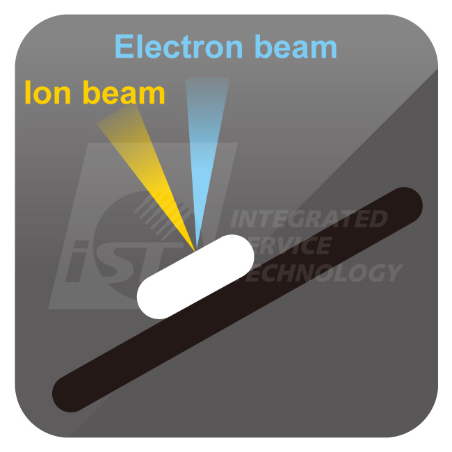
Focused Ion Beam (FIB) cross-sectioning is a precise technique used to reveal the internal structures of materials at the nanoscale. It involves the following key aspects:
- Ion Beam Milling: A focused ion beam is used to precisely remove material, creating a clean cross-section.
- Nanometer-Scale Precision: The ion beam allows for highly accurate material removal, revealing intricate subsurface features.
- Targeted Analysis: Specific areas of interest can be precisely examined for defects, interfaces, and microstructures.
FIB Cross-Sectioning Process at iST
Our process is structured into three key steps. By following this structured approach, iST ensures that clients receive high-quality, reliable data essential for materials analysis and failure investigation.
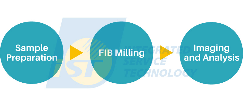
- Sample Preparation : Meticulous handling, including cleaning, mounting, and coating, ensures accurate cross-sectioning through proper alignment of the target area.
- FIB Milling : Using state-of-the-art FIB systems, we precisely remove material with a focused ion beam to create accurate cross-sections without damaging surrounding areas.
- Imaging and Analysis : Using Scanning Electron Microscope (SEM), we analyze the milled cross-section to gain detailed insights into the sample’s internal structures, allowing for accurate assessment of material properties, defect detection, and identification of failure points.
Benefits of FIB Cross-Sectioning
The FIB method offers several key advantages:
- High-Precision Analysis: Provides a detailed view of nanoscale structures, helping identify defects that could compromise material performance or product reliability.
- Real-Time Feedback: Quickly delivers internal structure imagery, accelerating failure analysis and supporting rapid process improvements in manufacturing and research.
- Accurate Localized Sampling: Enables precise cuts in small, targeted areas without damaging nearby structures, ideal for analyzing advanced packaging and nanoscale components.
- Multifunctional Operation: Beyond milling, FIB systems can perform ion beam deposition or etching. When combined with other analytical tools, this offers a comprehensive, one-stop analysis service.
- Sample Preparation Advantage: Produces thin, uniform samples suitable for Transmission Electron Microscopy (TEM), significantly enhancing efficiency in semiconductor R&D and other high-tech applications.
Applications of FIB Cross-Sectioning
- ICs Defect Analysis and Failure Investigation
- Microstructural Examination
- Development of Advanced Materials and Analysis
- Fabrication of Nanoscale Structures
- Characterization of Nanomaterials
Explore the Potential of FIB Cross-Sectioning with iST
FIB cross-sectioning leads materials analysis and failure detection with unmatched precision. Its ability to expose subsurface structures makes it indispensable for researchers and engineers. By using FIB, industries can boost product reliability, accelerate innovation, and better understand material properties.
Especially in the semiconductor industry, FIB cross-sectioning is crucial for advanced process nodes, enabling engineers to precisely analyze defects and validate designs at the nanoscale. With its ability to uncover intricate subsurface structures, FIB plays a key role in ensuring product reliability and accelerating innovation. With over 20 years of experience, iST offers fast, accurate defect detection and comprehensive FIB cross-sectioning services to meet your needs.
iST Material Analysis Laboratory has been working in the semiconductor and advanced packaging fields for a long time and has accumulated considerable experience and successful cases. If you have any related needs or want to further understand the relevant knowledge, please feel free to contact Mr. Weijui Lin at +886-3-579-9909 ext. 6166 or email at web_ma@istgroup.com;marketing_tw@istgroup.com。