Issued Date:2024/06/14
Issued By:iST
The terminology, TEM, has been mentioned a lot in the field of nanomaterials and the semiconductor industry daily in the 21st century. What does TEM mean? It is an acronym of either “Transmmion Electron Microscopy” or “Transmmion Electron Microscope”. The former means advanced techniques for material analysis. The latter means a powerful instrument to perform works of material analysis.
Traces of dislocations
Today, TEMs have been the most efficient and versatile instrument for nano-materials characterization, including morphology, crystal structure, and composition. They have become indispensable tools for R&D in semiconductor devices of nano-scale. iST has been a loyal partner for assisting reliability analysis (RA), failure analysis (FA), and material analysis (MA) for semiconductor manufacturers and relevant semiconductor companies for 30 years. Recently, iST has been reinforcing investment in the business of TEM analysis to assist global semiconductor corporations in developing high-end semiconductor products.(read more: Five Case Studies Unveil What You Don’t Know About TEM Material Analysis)
The first TEM, with a resolution of 50 nm, was built by Dr. Ernst Ruska in 1933, and Ruska received the Nobel Prize for this invention in 1986. The first commercial TEMs were developed in the UK in 1936. A TEM, with a resolution of 10 nm, was produced by Siemens and Halske in Germany in 1939. TEMs became widely available from several other sources, including RCA, Philips, Hitachi, and JEOL, after the end of World War II. The first TEM with a Cs corrector was built by Philips in Germany in 1998. This auxiliary improved the resolution of TEM to be better than 1Ǻ. However, a fly in the ointment for TEM is that its price is rising with its functions and resolution power.
1. Understanding TEM
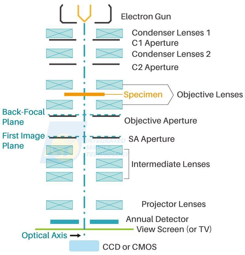
Figure 1. A schematical diagram shows the basic configuration of a typical modern TEM/STEM system [1].
(Source: iST)The basic configuration of a modern typical TEM/STEM system is shown schematically in Figure 1[1]. The essential components include an electron gun module, condenser lenses, objective lenses, intermediate lenses, projector lenses, annual detector(s), view screen (or TV), and CCD or CMOS. All components are integrated into a high to ultra-high vacuum system. The key component of a TEM is the objective lens which determines the resolution power of the TEM. Currently, the typical resolution is around 0.16 nm in TEM and STEM modes. The resolution can be further improved to around 0.05 nm when installing spherical aberration correctors.
Chemical analysis can be performed by installing accessory equipment, such as EDS and/or EELS. Current analyses of EDS and EELS are usually carried out in STEM mode. A spatial resolution of 1 nm is routinely available for most STEMs. Qualitative analysis is the first step analysis to identify what elements are in the interested region and roughly approximate composition of this region. The quantitative analysis gives the further accurate composition to a certain accuracy, such as 10%, 5%, or 2%, by further calculation. An EDS standardless quantitative analysis technique for using k factors [2, 3] instead of standard specimens has been developed and widely used in all built-in software in current TEM/STEM systems.
2. How Transmited Electron Microscope Works
Hundreds of kinds of materials, including metals, fine ceramics, semiconductors, and …, are being analyzed by TEM. Several techniques are used to prepare specimens of different materials. Among them, focus ion beam (FIB) has been the main technique for TEM sample preparation in TEM laboratories mainly dealing with semiconductor devices, due to its characteristic of high accuracy, high efficiency, and high yield rate.
A suitable protection layer, which keeps the morphology and the crystal structure of the top surface of the specimen, is first coated upon the specimen. After being put into the FIB, a slab containing interested features is dug from the chip and welded to a grid, then it is milled and polished (by low energy and low dose ions) to be a thin foil containing the feature structure.
This prepared thin foil is then loaded into TEM after plasma cleaning. Specimens of semiconductor devices are usually tilted to a specified zone axis, such as Si [1 1 0] or GaN [1 1 -2 0], for following TEM analyses. Data of images, electron diffraction patterns, and spectra are acquired at the correct mode and condition to meet what is required by customers.
Types of TEMs
Traditionally, TEMs were divided into three types: conventional TEM (CTEM), high-resolution TEM (HRTEM), and analytical TEM (AEM), as shown in Figure 2. CTEMs offer diffraction and image analysis, HRTEMs resolve the atomic structure of materials, and AEMs, which are STEMs, reveal chemical information about materials.
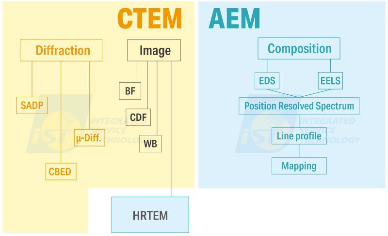
Figure 2. Traditional categories of TEMs and their analytical techniques are available.
(Source: iST)Today, the progress of precision machining and computer control has merged them into a TEM/STEM system that can perform all analyses mentioned, as shown in Figure 3, and all data (images, patterns, spectra) are stored digitally. Several new techniques have been developed by auxiliary of a high-performance computer which replaces a microprocessor in TEM operation.
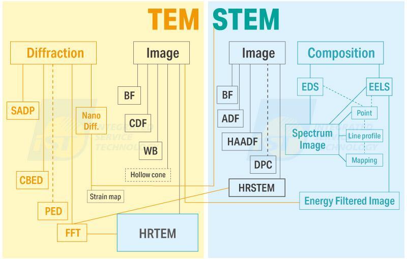
Figure 3. Analytical techniques of modern TEM/STEM systems.
(Source: iST)Spectrum image is a breakthrough technique for composition analysis after replacing microprocessors with computers. EDS and/or EELS spectra are collected simultaneously during image scanning in STEM mode. All chemical data, such as positions/line profiles/maps, of the interested features in the specimen can be offline extracted from the file whenever needed. This method saves lots of in-line operation time and promotes the rate of instrument utilization.
Applications of TEMs
Properties of materials and devices of nanotechnology depend deeply on their microstructure. The more detail we understand the microstructure, the more precisely we can manipulate the properties of the materials and devices. Current semiconductor devices, including the 1st generation to the 4th generation, consist of many thin film structures of several nanometers to sub-nano meters. TEM reveals both microstructure and composition to nano and atomic scales accurately and routinely. (Read More: How to Identify & Analyze Ga2O3?)
3. Why Choose iST for Your TEM Analysis Needs
There are three TEM laboratories in the Taiwan MA market, what advantages of choosing iST? Besides well-trained technicians and sophisticated instruments, iST has an MA TEM management team with a well-educated and experienced crew, including more than 15 postgraduates, to communicate with customers and to understand what kinds of data customers need exactly.
TEM can reveal microstructure information of materials and semiconductor devices to nanometer and atomic scale. This kind of microstructure information can help researchers and engineers to progress their work efficiently and effectively. However, the cost of setting up TEMs and keeping them in operation routinely is very high today. iST can help you to extract these useful data with an affordable budget.
References:
[1] J. W. Edington, in Practical Electron Microscopy in Materials Science, Van Nostrand Reinhold Company, New York (1976). ISBN: 0-442-22230-0
[2] Cliff G. and Lorimer, G. W., J. Microscopy, 103, p.203 (1975).
[3] David B. Williams and C. Barry Carter, in Transmission Electron Microscopy, Microscopy, part 2, Plenum Press, New York (2007). ISBN: 0-471-122440-0