
Issued Date:2026/10/06 Hotspot Tool
Issued By:iST
When an IC exhibits an electrical abnormality, one of the first priorities for failure analysis engineers is to quickly and accurately locate the hotspot associated with the failure. However, with several hotspot localization techniques available, how do you select the right tool without wasting valuable analysis time or risking further damage to the sample?
Based on extensive hands-on experience at iST’s Electrical Failure Analysis (EFA) laboratory, one of the most common challenges engineers face is selecting the appropriate localization technique according to the electrical characteristics of the failed device.
In this edition of iST Classroom, we explain how InGaAs, OBIRCH, Thermal EMMI, and QDm can be applied to four major electrical failure modes—leakage, high resistance, short circuit, and open circuit—helping engineers efficiently pinpoint defects while saving time, effort, and analysis cost.
Hotspot Tool
Hotspot Tool
I. Identify the Four Major Electrical Failure Modes Using I-V Curve Analysis
When an IC does not operate as designed, the first step is to characterize the abnormal pin using a parameter analyzer and I-V curve measurement.
By comparing the current-voltage characteristics of a known-good device with those of the failed device, as illustrated in Figure 1, electrical abnormalities can generally be categorized into four major failure modes.
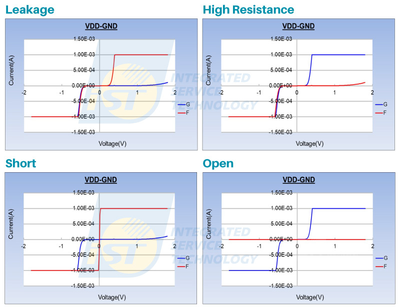
Figure 1: Schematic I-V curve comparison for identifying IC electrical failure modes (blue: good device [G]; red: failed device [F]).
(Source: iST)1.Leakage
Leakage is characterized by abnormally high current under the normal operating voltage, indicating the presence of an unintended leakage path within the device.Typical causes include gate oxide breakdown and PN junction leakage. Although the device may not yet be in a complete short-circuit condition, excessive leakage can significantly increase power consumption and generate abnormal heat.
2.High Resistance
A high-resistance condition is characterized by lower conduction current than that of a normal device, with the I-V curve typically shifting toward a higher voltage.
This indicates excessive resistance along the electrical path, meaning that a higher voltage is required to drive even a small amount of current.
Common causes include poor via/contact integrity, metal-line microcracks, voids, and cold solder joints.3.Short Circuit
A short circuit occurs when the resistance between two nodes—for example, VDD and GND—approaches zero.
Under this condition, the two nodes become directly conductive and the intended switching or gate-control function is effectively lost. Even a very small applied voltage can therefore result in excessive current.
Common causes include metal bridging, ESD-induced breakdown, and dielectric pinholes.4.Open Circuit
An open circuit occurs when an electrical path is completely disconnected, resulting in extremely high or effectively infinite resistance and preventing current from flowing through the circuit.
Typical causes include bump delamination, broken bonding wires, and completely ruptured or burned-out metal interconnects.II. Choosing the Right Tool for Each Electrical Failure Mode
Once the failure mode has been identified through I-V curve analysis, the next step is to select the appropriate localization technique.
Every hotspot localization tool has its own strengths and limitations. Based on years of practical EFA experience, iST’s Electrical Failure Analysis team has developed the following tool-selection strategy to help engineers identify defects more efficiently.1. Leakage: Start with InGaAs
When an IC exhibits leakage, InGaAs emission microscopy is typically our first choice.
(1)Why Choose InGaAs First?
InGaAs detectors are highly sensitive to weak near-infrared photon emissions generated by electrical activity inside semiconductor devices.
Under an applied bias, leakage-related defects may generate weak photon emissions through mechanisms such as electron-hole recombination. InGaAs analysis can capture these emissions and visualize their locations as hotspots, making it particularly effective for localizing leakage-related defects.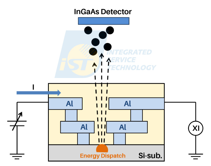
Figure 2: Schematic illustration of hotspot detection using InGaAs
(Source:iST)(2)When Should Other Tools Be Considered?
Thermal EMMI (InSb) or OBIRCH may be more suitable when:- The package cannot be decapsulated or otherwise prepared for optical access.
- Leakage current is sufficiently high that the resulting thermal effect dominates over photon emission.
- The device incorporates a stacked-die or other complex multilayer structure.
(3)iST Recommendation
If backside access or backside thinning is feasible, Backside InGaAs analysis is recommended as the first-line approach, as it generally provides a higher probability of successful localization together with better spatial resolution.
For intact packages that must remain non-destructive, Thermal EMMI can first be used to identify the approximate thermal region, followed by X-ray analysis to correlate the hotspot with the internal package structure.(4)Case Study
Under applied bias, the failed device exhibited abnormal leakage current. After backside thinning, InGaAs analysis was performed.
The detector rapidly captured weak photons emitted through electron-hole recombination at the defect sites, revealing several distinct hotspots. These locations subsequently provided precise coordinates for FIB cross-sectioning and TEM-based physical failure analysis (PFA).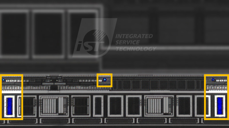
Figure 3: Leakage localization using InGaAs emission microscopy.
(Source: iST)2. High Resistance: Start with OBIRCH
When an IC exhibits a high-resistance abnormality—such as increased contact/via resistance or a metal-line microcrack—OBIRCH (Optical Beam Induced Resistance Change) is typically the preferred first-line technique.
(1)Why Choose OBIRCH First?
OBIRCH uses localized laser heating to induce changes in resistance along an electrically biased circuit. By monitoring the resulting current variation (ΔI), the system can identify locations where abnormal resistance behavior occurs.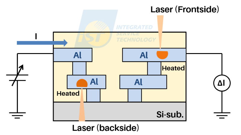
Figure 4. Schematic illustration of hotspot detection using OBIRCH
(Source: iST)Depending on the sample structure, OBIRCH can support both frontside and backside scanning. For frontside analysis, the laser can directly illuminate exposed die surfaces or accessible upper metal structures. If dense frontside metallization blocks optical access, the silicon substrate can be thinned for backside analysis.
A 1300 nm laser provides good transmission through silicon, allowing localized heating to reach underlying structures and helping identify resistive defects within deeper interconnect layers.(2)When Should Other Tools Be Considered?
If a high-resistance defect is approaching a complete open circuit, the available current variation (ΔI) may become extremely small.
Similarly, in advanced packaging structures such as CoWoS or multilayer RDL architectures, optical access may be restricted.
Under these conditions, simply increasing the applied voltage in an attempt to enhance the signal can be risky, as the already weakened interconnect may be permanently burned open.(3)iST Recommendation
For high-resistance failures, safe current control is critical.
We recommend beginning with low-power OBIRCH scanning. For advanced packages or high-resistance failures involving deeply embedded multilayer interconnects, QDm (Quantum Diamond Microscopy) can be considered.
By sensing magnetic fields generated by electrical current, QDm can reconstruct the current path and is less susceptible to limitations associated with optical obstruction and thermal spreading.(4)Case Study
Under the same applied bias, the known-good device (Figure 5, left) exhibited the expected activation signals, while the failed device (Figure 5, right) showed only a very small abnormal current, indicating excessive resistance that restricted normal current flow.
Backside OBIRCH analysis revealed that the normal thermally induced signal within the highlighted region had completely disappeared in the failed device.
Subsequent delayering analysis could then focus on this specific region to precisely identify the physical defect.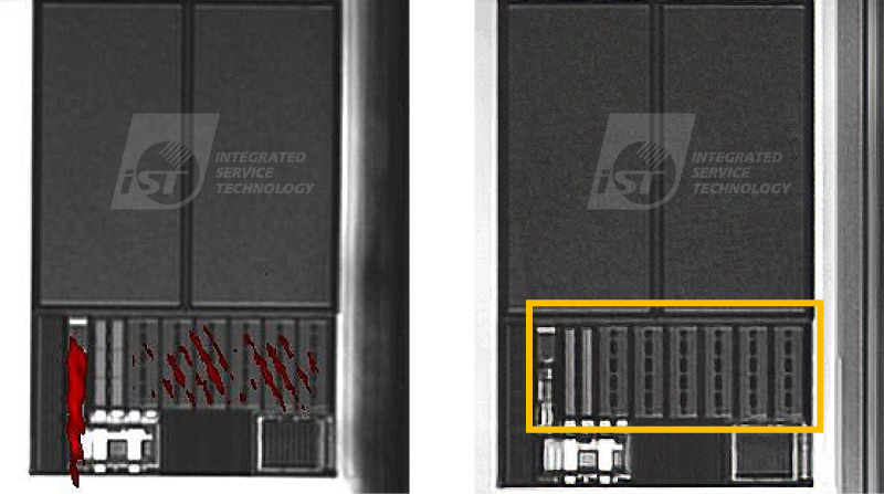
Figure 5. High-resistance defect localization using OBIRCH.
(Source: iST)3. Short Circuit: Start with OBIRCH or Thermal EMMI (InSb)
For IC short-circuit failures, OBIRCH or Thermal EMMI (InSb) is typically selected according to the electrical behavior, sample structure, and magnitude of the short-circuit current.
(1)Why Choose OBIRCH or Thermal EMMI?
When the short occurs within the chip’s metal interconnect layers—for example, due to a metal bridge or dielectric pinhole—localized laser heating can induce a significant change in resistance and current (ΔI).
OBIRCH provides high spatial resolution and can therefore be highly effective in pinpointing micron-scale short-circuit locations.
For high-current shorts, significant Joule heating can occur even at very low applied voltages.
Thermal EMMI using an InSb detector can detect thermal infrared radiation in approximately the 3.0–5.0 μm wavelength range, enabling rapid localization of heat-generating defects.
One major advantage is that Thermal EMMI can be applied to intact packages or PCB assemblies without decapsulation, making it particularly useful for rapid non-destructive screening.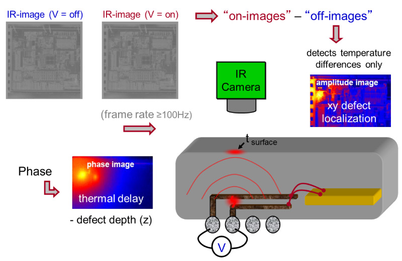
Figure 6: Schematic illustration of hotspot detection using Thermal EMMI (InSb).
(Source: Thermo Fisher)(2)When Should QDm Be Considered?
For buried shorts inside advanced packaging structures such as CoWoS, 3D ICs, HBM, or multilayer RDLs, conventional optical or thermal techniques may face significant limitations.
The OBIRCH laser may be unable to access the target structure through multiple layers, while Thermal EMMI may suffer from thermal spreading, resulting in a broad, blurred thermal signature that cannot accurately resolve the defect location or its depth along the z-axis.
In such cases, QDm can provide an alternative approach.(3)iST Recommendation
For relatively small bare-die samples or localized short-circuit failures, OBIRCH is generally preferred.
For packaged devices or high-current direct shorts, Thermal EMMI can first be used for coarse hotspot localization.
For advanced packages or regions containing multiple stacked metal layers, QDm is recommended for non-destructive magnetic-field-based current-path reconstruction, helping engineers visualize current flow through complex structures.(4)Case Study 1: Short Localization with OBIRCH
Under the same applied bias, the failed device (Figure 7, right) exhibited a short-circuit abnormality.
Backside OBIRCH analysis detected an abnormal hotspot within the highlighted region, where the image also suggested possible metal melting or electrical overstress damage.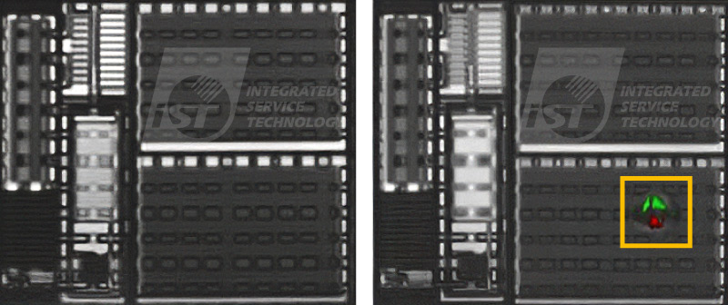
Figure 7: Short-circuit localization using OBIRCH (left: good device; right: failed device).
(Source: iST)(5) Case Study 2: Non-Destructive Localization with Thermal EMMI
Without decapsulation, voltage was applied to the failed device and Thermal EMMI detected an abnormal heat source within the highlighted region.
The Thermal EMMI image was subsequently correlated with X-ray imaging to determine whether the heat source originated from the package structure or the die.
This combined approach helps engineers select the appropriate subsequent FA technique while reducing the time lost to unsuitable analysis methods.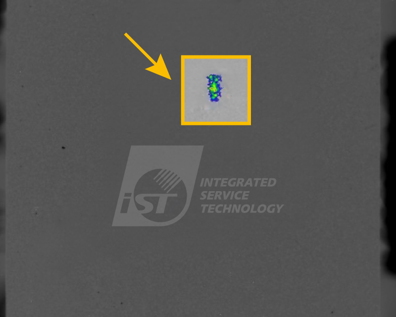
Figure 8: Short-circuit localization using Thermal EMMI (InSb).
(Source: iST)(6)Case Study 3: BGA Package Hotspot Localization
Figure 9 shows a BGA-packaged IC with a distinct hotspot near the center of the package.
Without opening or decapsulating the package, voltage was applied to the abnormal pin to induce localized heating. Thermal EMMI successfully captured the resulting thermal radiation and identified the hotspot.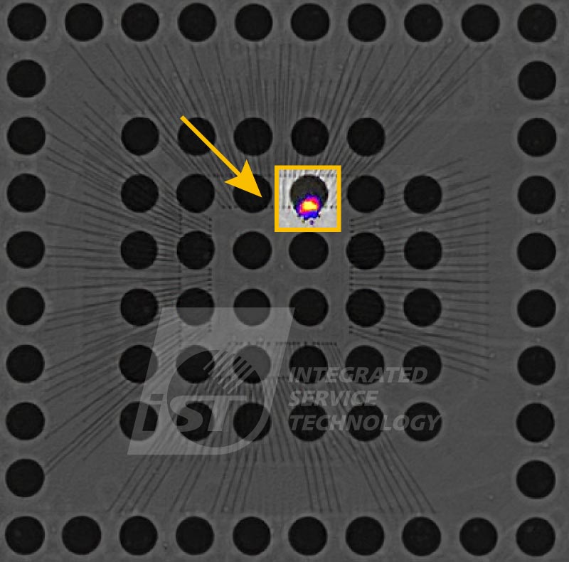
Figure 9. Short-circuit hotspot localization in a BGA-packaged IC using Thermal EMMI.
(Source: iST)(7)Case Study 4: Driver IC and Panel Interconnect Failure
Figure 10 shows a case involving a microcrack or localized short within the interconnect or bonding region between a driver IC and a display panel.
Once electrically biased, the abnormal current path generated localized heat. Thermal EMMI was used to identify the heat source, followed by PCB X-ray imaging to inspect the internal structure.
By combining electrical localization with physical verification, engineers can establish a more efficient FA workflow.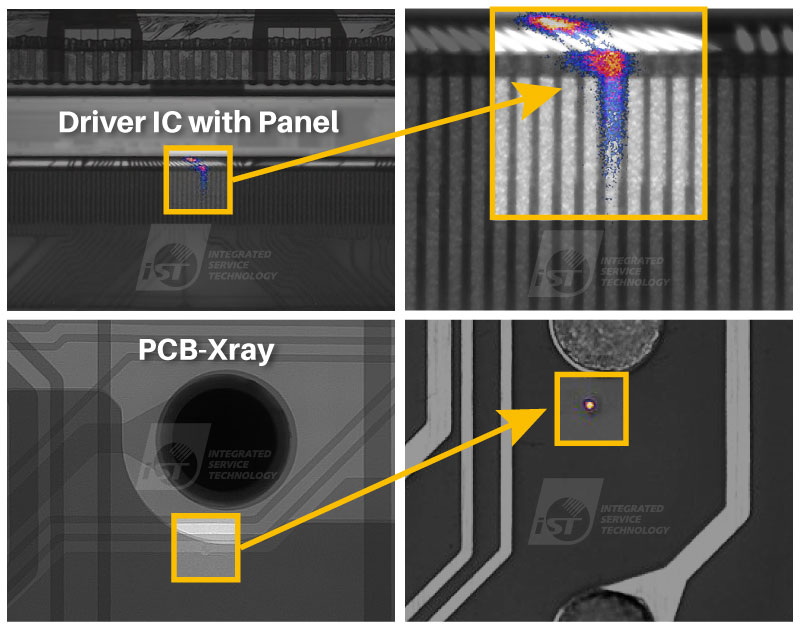
Figure 10: Top left/right: Localization of a heat-generating, low-resistance hotspot near the interconnect between the driver IC and panel. Bottom left: X-ray imaging reveals an internal via-related structural abnormality. Bottom right: Thermal EMMI identifies localized heating along the PCB interconnect.
(Source: iST)4. Open Circuit: Start with Comparative OBIRCH Analysis
Open-circuit failures are among the most challenging electrical failures to localize.
(1)Why Is Open-Circuit Analysis So Difficult?
A complete open circuit means that no continuous current path is available for conventional electrical sensing.
As a result, techniques that depend on current-induced photon emission, such as InGaAs emission microscopy, or on laser-induced current/resistance changes, such as conventional OBIRCH, may become ineffective.(2)How Can an Open Circuit Be Localized?
Whenever possible, iST recommends providing both a known-good device and a failed device for comparative analysis.
Engineers can first identify normal activation or response locations in the good device and then compare them with the failed device to identify missing or abnormal responses.i.Method 1: High-Voltage/High-Frequency Excitation (RF/AC Bias) + OBIRCH
By applying a high-frequency AC signal, the parasitic capacitance across an open-circuit location may generate a small charging/discharging displacement current.
This weak electrical response can produce localized changes that may be detected and compared using OBIRCH-based analysis, helping narrow down the suspected open-circuit location.ii.Method 2: Magnetic-Field-Based Current-Path Reconstruction with QDm
For advanced 2.5D/3D packages or failures involving broken bumps or bonding wires, QDm provides a unique advantage by sensing extremely weak magnetic-field distributions generated by current flow.
By mapping the point at which the current-generated magnetic signature changes or disappears, engineers can visualize where the electrical current path is interrupted and thereby narrow down the location of the open defect.(3)When Should Physical Failure Analysis Techniques Be Used Instead?
If the electrical path is completely open and even high-frequency excitation cannot generate a detectable response, conventional EFA hotspot localization techniques may reach their practical limits.
In such cases, iST recommends switching to X-ray or 3D X-ray computed tomography (CT) for non-destructive structural inspection.
These techniques can directly reveal structural abnormalities such as broken bonding wires, bump separation, and via-related discontinuities.(4)iST Recommendation
When dealing with an open-circuit failure, engineers should avoid blindly increasing the DC voltage, as this may introduce secondary damage without improving localization capability.
Instead, first determine whether high-frequency or higher-voltage excitation can generate a measurable response. QDm can then be considered to identify discontinuities in the current-generated magnetic-field distribution.
If the device shows no usable electrical response, combining the analysis with 3D X-ray imaging is often the most efficient approach for saving both analysis time and valuable samples.(5)Case Study
A high-voltage or high-frequency AC bias was applied to the abnormal pin.
The weak displacement current associated with the parasitic capacitance across the open-circuit location, together with the corresponding electromagnetic-field variation, was then used to narrow down the suspected discontinuity.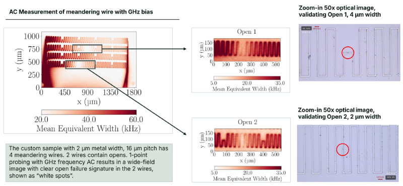
Figure 11: Open-circuit localization using high-frequency AC bias combined with laser/thermal sensing techniques.
(Source: QuantumDiamond)
If you have any questions about selecting the right analysis tool for the four major electrical failure modes, feel free to contact us for our recommended tool selection guide.
For further assistance, please contact Ms. Chen at +886-3-579-9909 ext. 1065 or email marketing_tw@istgroup.com. We will connect you with the right technical experts to address your failure analysis needs.