
Issued Date:2026/07/14 cowos open
Issued By:iST
cowos open
cowos open
In the era of advanced packaging technologies like CoWoS and 3D ICs, are you, as a Failure Analysis (FA) engineer, trapped in this frustrating cycle: “The chip is failing; we can clearly detect the Short, but the Open defect remains completely untraceable!”
Undeniably, traditional 2D electrical localization tools—such as InGaAs, OBIRCH, and EMMI—remain powerful and indispensable weapons for handling shorts and leakage currents in planar (2D) chips.
However, when facing intricate 3D stacked structures, these conventional tools can only “hint or guess” at shorts via Hot Spots underneath the silicon. Affected by the chip’s metal layers or packaging materials, the thermal energy dissipates into a blurry cluster. It becomes practically impossible to distinguish which specific anomaly point lies beneath that heat blob, driving engineers to despair.
Three Major Bottlenecks of Traditional 2D Electrical Localization in 3D Structures:
1.Misleading Hot Spots:
Thermal dissipation caused by material properties often distorts the hot spots detected by optical systems, making it impossible to precisely pinpoint a single failure location or lock onto a specific layer.
2.Signal Interference:
Structural crosstalk and buried defects between stacked die layers frequently mask the true root causes.
3.Insufficient Information:
Traditional front-side and back-side imaging techniques only provide two-dimensional (X, Y) anomaly data, which falls short of the precise 3D (X, Y, Z) localization required for multi-layer packaging.
In the past, FA engineers had to rely on experience and pure luck for “blind cross-sectioning.” This dilemma was not only time-consuming and low in success rate, but it also severely dragged down the R&D and time-to-market schedules for new products.
The Solution is Here! Perfectly Complementing Traditional Tools to Redefine Advanced Packaging Diagnostics
To solve this industry pain point, iST has taken the lead by teaming up with QuantumDiamonds—a next-generation anomaly localization equipment manufacturer from Germany. Together we have launched Asia’s very first “Quantum Diamond Microscope (QDm)” Demo and verification service in Taiwan!
Distinct from traditional tools, the core principle of QDm utilizes billions of Nitrogen-Vacancy (NV) centers within a diamond to convert magnetic field gradients into optical signals. By detecting “magnetic fields and electric currents,” it non-destructively penetrates packaging materials. Combined with layout information, QDm achieves “complete visualization of the current path.” Not only can it clearly observe Short circuits, but it can also precisely locate the once-unsolvable “Open” circuits and high/low resistance anomalies, thereby accelerating decision-making.
Furthermore, QDm can collaborate with traditional electrical tools. It can precisely overlay the blurry yet valuable Hot Spots measured by traditional tools directly onto the “sharp metallic routing” captured by QDm. This allows engineers to instantly lock onto the most suspicious metal line, leading to highly accurate physical failure analysis (PFA) cross-sectioning and a soaring sample preparation success rate.
Quantum-Level 3D Failure Localization: Powerful Specifications at a Glance
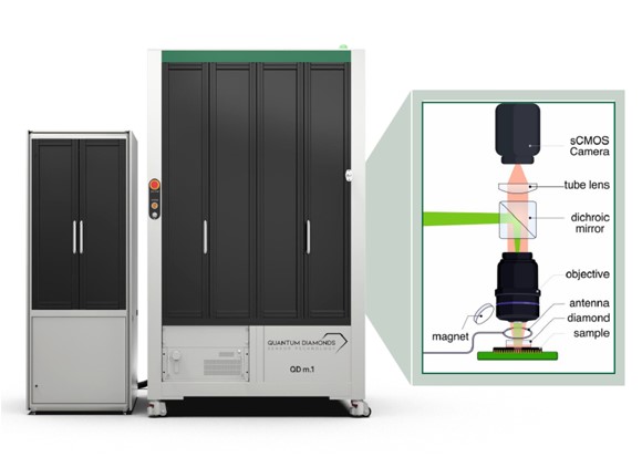
Figure 1: Internal Schematic Diagram of the Quantum Diamond Microscope (QDm)
(Source:QuantumDiamonds)
- High-Precision Localization: XYZ localization accuracy down to 1.4 μm.
- Extreme Sensitivity: Sensitive down to 100s nA
- Wide Field of View & High Efficiency: Features a wide 3 mm x 3 mm field of view (FOV), with an average measurement time of just 5 minutes!
💡 Want to experience the power of quantum verification firsthand and drastically boost your chip R&D failure analysis success rate?
Asia’s only Demo Tool verification slots are now open for limited bookings! Whether it is high/low resistance opens and shorts, or wide-bandgap semiconductors like Silicon Carbide (SiC) and Gallium Nitride (GaN), QDm will be your ultimate asset!
To arrange a product demonstration or discuss your sample verification needs, please contact Ms. Chen at +886-3-579-9909 Ext. 1065 | Email: marketing_tw@istgroup.com