
Issued Date:2026/8/21 Large BGA rework
Issued By:iST
High-end AI server chips (CoWoS/EMIB) can cost over $30,000! Scrapping one over a solder defect is an R&D budget nightmare. Safely removing the chip, cleaning the board, and then precisely remounting it remains a massive technical hurdle.ation? Furthermore, how can R&D engineers bridge the standard gap to ensure products successfully pass the bring-up phase and transition into smooth mass production?
Large BGA rework
Large BGA rework
With the explosion of Generative AI, and Large Language Models (LLMs), flagship server chips like NVIDIA’s Blackwell series (e.g., B200), the Ultra series, as well as high-end chips from AMD and Intel, rely heavily on 2.5D / 3D heterogeneous integration advanced packaging technologies.
To push the boundaries of computing performance, chips are no longer single silicon dies. Instead, CPUs, GPUs, and multiple High Bandwidth Memory (HBM) stacks are integrated together on a single package. This causes the total footprint of the finalized chip package to expand exponentially, easily exceeding 90 × 90 mm—a size unimaginable in traditional consumer electronics, where smartphone chips typically top out around 15 × 15 mm.
When a multi-thousand-dollar AI chip fails testing at the final printed circuit board assembly (PCBA) stage due to soldering defects (such as cold solder joints or bridging), scrapping the entire board is financially painful. This is precisely where a high-precision “Rework System” steps in. Safely removing the expensive chip, thoroughly cleaning the PCB, and accurately re-soldering it back on represents an extraordinarily high engineering barrier.
Facing the physical challenges of massive chip sizes, the industry-standard IPC-9701 specification (Reliability Test Methods for Surface Mount Solder Attachments) has become increasingly stringent. Covering key steps from initial assembly to rework, this standard is a critical benchmark for ensuring AI servers operate reliably without field failures under high-temperature and high-load environments.
This article explores how a specialized solution can overcome physical equipment limitations, ensure high yield, and deliver a reliable “Large-Scale IC Mounting and Auto-Rework Solution” to assist the AI supply chain in conquering the final mile of hardware evolution.
I. Manufacturing Bottlenecks Driven by Massive AI Server Chips
In recent validation support for our clients, iST frequently observes a common industry pain point: “What systems can be used to mount today’s extra-large chips (up to 150 × 150 mm)? And during chip rework, how can quality be ensured?”
1. Size Limitations of Standard Pick & Place (P&P) Equipment
Mainstream Pick & Place (P&P) machines are physically constrained, typically handling components up to 90 × 90 mm. Confronted with today’s massive AI chips exceeding 90 × 90 mm, standard production line equipment falls short of meeting precision alignment and placement demands.
2. Risks Associated with Manual Rework
When oversized chips require rework or repair, using conventional manual hot-air guns or non-specialized heating equipment frequently introduces severe defects:
(1)PCB Peeling / Delamination:
Non-uniform heating or excessive local thermal stress damages the laminated structure of the PCB (Printed Circuit Board).(2)Component Scorching & Cold Solder Joints:
Imprecise temperature control burns component surfaces or leaves solder paste incompletely reflowed, forming cold solder joints that compromise connection integrity.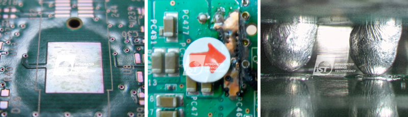
Figure 1: Common defects in traditional manual de-soldering due to imprecise temperature control: Board pop/delamination, component scorching, and cold soldering (left to right).
(Source: iST, created with AI assistance)(3)Pad Defects & Damage:
Manual solder removal using traditional physical wicking or scraping easily scratches or tears off delicate circuit board pads.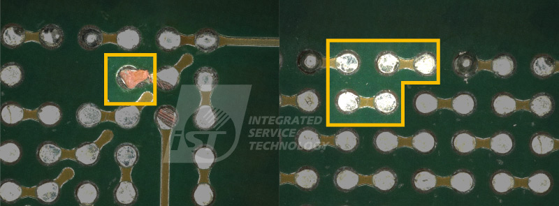
Figure 2: Common defects during traditional manual rework. Left: BGA pad damage. Right: Non-uniform solder height after manual solder removal.
(Source: iST, created with AI assistance)II. The Solution: High-End Rework Systems & Automated Non-Contact De-soldering
To break through the bottlenecks of mounting and reworking oversized chips, iST has introduced a high-precision rework system tailored specifically for large-scale packages. By combining advanced thermal management with high-resolution optical alignment, this solution ensures reliable BGA removal, placement, and rework without thermal or physical damage.
1. Extra-Large Component Handling Capacity
Equipped with a specialized XL heating head, the system effortlessly processes components up to 150 × 120 mm, comfortably surpassing the 90 × 90 mm threshold of next-generation AI chips.
2. High-Precision Optical Alignment
Featuring a 5 MP GigE high-resolution color camera, the system uses Optical Superposition to fine-tune Theta rotation and X/Y-axis offsets, achieving placement accuracy within ±25 μm.
3. Customized High-Power Hybrid Thermal Control
Utilizing high-power Bottom Infrared (IR) combined with Top Hot-Air convection heating, integrated with a Real-Time Profile monitoring system (expandable up to 7 thermocouple channels), the system ensures uniform heat distribution across large substrate areas to prevent board warpage or scorching.
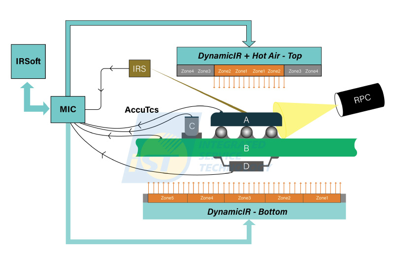
Figure 3: Schematic of the hybrid heating architecture combining high-power Bottom Dynamic IR with Top Hot-Air convection.
(Source: Kurtz Ersa, remade by iST)4. Non-Contact Auto Scavenger (Automatic Solder Removal)
Once the BGA component is lifted, the automated cleaning nozzle lowers to clean the residual solder in a completely non-contact manner relative to the PCBA. This entirely eliminates pad damage caused by manual scraping.
III. Case Studies
In iST’s laboratories, high-value AI server motherboards carrying massive chips are frequently submitted for urgent rework or assembly validation. To demonstrate how high placement precision and zero-damage repair are achieved simultaneously, below are practical case workflows:
Case 1: Precision Optical Alignment & Mounting for Large Chips
(> 90 × 90 mm)- Customer Challenge:
A customer developed a giant AI chip that standard SMT lines could not accurately place, while fearing that uneven reflow heating would ruin the high-cost component.
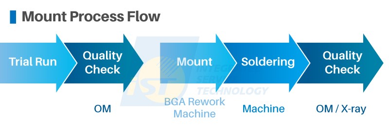
Figure 4: Workflow for mounting large chips (> 90 × 90 mm).
(Source: iST)1. Precision Optical Superposition Alignment
During alignment, the 5 MP GigE camera projects images of the chip pins (highlighted in orange in figure 5 and 6) and the PCB pads (highlighted in green in figure 5 and 6) onto the same screen simultaneously using beam-splitter optics. Engineers can intuitively adjust the Theta angle (rotational correction) and X-Y axes (linear alignment) to achieve placement accuracy within ±25 μm. Once aligned, the vacuum nozzle releases the component onto its exact target coordinates safely.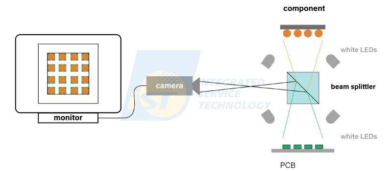
Figure 5: Principle of Optical Superposition alignment. The system utilizes a beam splitter and dual LED illumination to capture images of top chip pins (orange dots) and bottom PCB pads (green squares) concurrently, overlapping them on-screen for intuitive and accurate micro-adjustments.
(Source: Kurtz Ersa, remade by iST)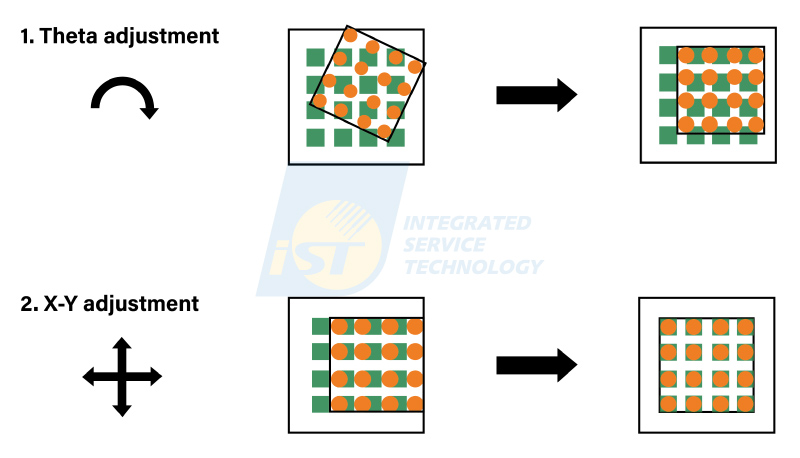
Figure 6: Alignment correction mechanism. The system executes a two-stage correction post-image overlap: 1. Theta adjustment (rotational angle alignment) and 2. X-Y adjustment (horizontal linear alignment) to ensure perfect matching between solder balls and PCB pads.
(Source: Kurtz Ersa, remade by iST)2. Real-Time Multi-Point Thermal Profile Monitoring
During reflow, high-power IR combined with hot-air heating is monitored via multiple (up to 7) thermocouple wires attached directly across the board. The system draws dynamic real-time temperature profile curves on-screen, guaranteeing even thermal distribution across all corners of the giant package to eliminate warpage, scorching, or cold soldering.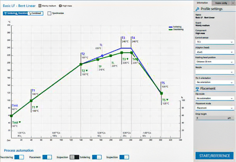
Figure 7: Real-time thermal profile monitoring using up to 7 thermocouple probes during operation, ensuring uniform heating across giant substrates to prevent warpage.
(Source: Kurtz Ersa, remade by iST)Case 2: Damage-Free Rework of High-Value Large BGA Components
Following functional testing on an AI server board, a large BGA required replacement due to solder joint defects. The customer’s primary concern was that manual solder removal on the substrate would scratch or tear off fragile pads, causing a multi-thousand-dollar board to be scrapped.By applying automated, non-contact solder scavenging, the risk of pad scratching is reduced to zero, leaving a pristine substrate surface ready for clean re-mounting of the new component.
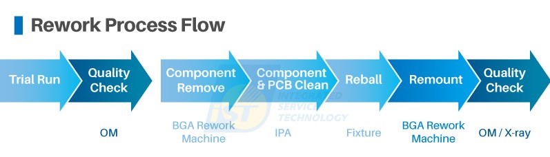
Figure 8: BGA component rework and repair workflow.
(Source:iST)1. Automated Non-Contact Solder Removal (Auto Scavenger)
After the system automatically de-solders and lifts the defective chip, uneven residual solder remains on the board. The Auto Scavenger module activates automatically without requiring time-consuming manual setup. The vacuum nozzle hovers just above the board surface, extracting residual solder rapidly with zero physical contact with the PCBA.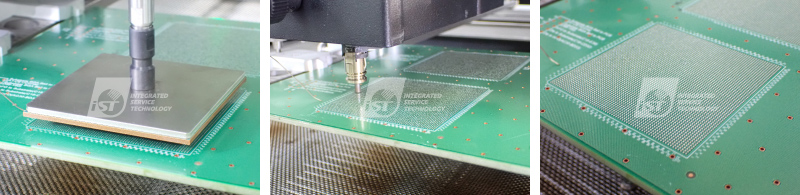
Figure 9: Non-contact automated de-soldering sequence (left to right): BGA lifting, solder extraction, and completely cleaned pads.
(Source:iST)- Customer Challenge:
In the era of giant AI chips driven by 2.5D / 3D advanced packaging, a single soldering defect can mean a scrap crisis of over $30,000. Mastering the precise placement and damage-free rework of large-scale packages to effortlessly pass strict reliability standards—without hurting your budget or your circuit boards—is the ultimate key to succeeding in AI hardware evolution.
iST is pleased to share our verification and rework experiences with you. If you have any technical inquiries or would like to learn more about our large-scale IC mounting and BGA rework services, please feel free to reach out Ms. Chen at +886-3-579-9909 Ext. 1065 | Email: marketing_tw@istgroup.com We will connect you with our specialized technical team to address your inquiries!