Issued Date:2025/8/19 Kikuchi Bands EBSD
Issued By:iST
Did you know? In the world of materials analysis, electron microscopes don’t just “take pictures”—they can actually interpret how each crystal is arranged and oriented.
Kikuchi Bands EBSD
This technique is called EBSD (Electron Backscatter Diffraction). It decodes the orientation of crystals through a series of seemingly abstract but information-rich diffraction patterns. EBSD is not only a critical tool in academic research—it’s also widely used in advanced semiconductor packaging analysis, such as in Through Glass Via (TGV) and Hybrid Bump structures.
In a previous “iST Tech Library,” we discussed the importance of crystal structures in determining material properties and demonstrated how material analysis can be key to ensuring the reliability of advanced packaging. (read more: crystal structures in materials: the key to unbeatable semiconductor advanced packaging). This time, we’ll explain how EBSD works in a simpler and more intuitive way—from image capture and band recognition to indexing, and the key factors that affect accuracy. Step by step, you’ll discover how EBSD “reads” crystal orientations from diffraction patterns. Starting from the basic principles, we’ll show how EBSD uses Kikuchi bands to identify crystal orientations.
EBSD provides a way to truly “look into” materials. It helps engineers better understand process variation and potential risks by providing insights into grain orientation, boundary types, and residual stress.
First, in materials analysis, we often hear the term “crystal orientation.” Did you know the direction crystals line up can actually affect a metal’s mechanical strength, a semiconductor’s conductivity, and even whether a device might fail? This technique works by analyzing a series of electron diffraction patterns to reconstruct the orientation of each crystal—just like how a forensic expert can identify someone from their fingerprints, EBSD can deduce crystal orientation from electron diffraction patterns.
In this article, we’ll show you how EBSD can “understand” crystal orientation!
Kikuchi Bands EBSD
Kikuchi Bands EBSD
1.The Secret Behind the Patterns: What Are Kikuchi Bands?
When a high-energy electron beam hits the tilted surface of a sample, some electrons are scattered by the atoms inside the crystal. This interaction produces a series of light and dark lines, known as Kikuchi bands. The arrangement and angles of these bands serve as the fingerprint of a crystal’s orientation.
If you’ve ever seen light cast intricate patterns through a glass chandelier, you’ve witnessed an optical version of this effect. Kikuchi bands work in a similar way—but instead of light, they involve electrons interacting with a crystal’s internal structure.
2. Geometry of Bands ≠ Noise — They're Projections of Crystal Planes.
What makes EBSD special is that it doesn’t directly “see” the crystal; rather, it mathematically reconstructs it. Each Kikuchi band corresponds to a specific set of crystal planes, such as (100), (111), or (200). If at least three non-parallel bands can be identified, the crystal’s orientation can be deduced.
In other words, each diffraction pattern—called an EBSP (Electron Backscatter Diffraction Pattern)—is like a geometric message from the crystal. By interpreting the bands, we can determine the orientation of the crystal.
3. Decoding the Patterns: How do we determine crystal orientation from Kikuchi bands?
The EBSD system generally follows these steps to interpret Kikuchi bands (see Figure 1):
- Image acquisition: Capture the Kikuchi pattern using an EBSD detector.
- Band detection: Use mathematical models and algorithms to identify the position and direction of the bands.
- Indexing: Match the detected bands with a database of known crystal structures to determine orientation.
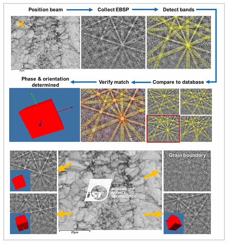
Figure 1. Workflow of EBSD: starting with the electron beam hiting the sample, the system captures the diffraction pattern (EBSP), then performs band detection and database matching, and finally extracts the phase and orientation information. (Image source: iST)
4. What Determines EBSD Accuracy?
Following three key factors can affect the accuracy of EBSD:
4-1 Scan resolution: If the electron beam scan step size is too large, small grains may be misinterpreted or overlooked, affecting the accuracy of grain size statistics. (see Figure 2).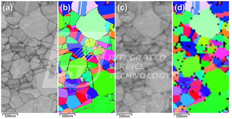
Figure 2. BC and IPF maps obtained with two different scan step size: (a) BC at 5nm scan step size, (b) IPF at 5nm scan step size, (c) BC at 50nm scan step size, (d) IPF at 50nm scan step size. (Image source: iST)
4-2 Band clarity: The sample surface must be extremely flat during preparation. Roughness, contamination, or oxidation—even minor scratches—can degrade the quality of Kikuchi bands, leading to unreadable or misinterpreted results.
In the images below, line-shaped and spot-shaped artifacts in the BC and IPF maps are caused by scratches and polishing residue, respectively. In some cases, both occur together. These scratches can cause slight lattice distortions that do not represent the true internal crystal structure, while foreign particles may be mistaken for secondary phases—necessitating additional elemental analysis and wasting time.
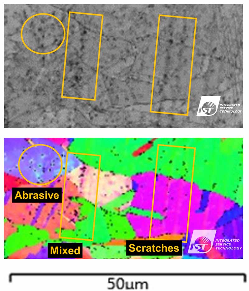
Figure 3. Effects of surface scratches and embedded polishing residue on BC and IPF maps. (Image source: iST)
4-3 Indexing Parameters: Incorrect material and structure parameters can lead to mis-indexing, preventing accurate phase identification. (see Figure 4).
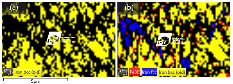
Figure 4. Phase maps using different imported phase data: (a) Map with only the α-iron phase imported, (b) Map with α-iron, γ-iron phase and Fe3C phases imported. (Image source: iST)
These conditions form the foundation for ensuring EBSD delivers stable and accurate data in real-world applications. Through diffraction pattern analysis and indexing, researchers can further investigate how crystal structure profoundly influences material properties.
Next in our iST Tech Library, we’ll dive into the practical applications of EBSD in TGV processes, including how EBSD helps correlate grain structures, residual stress, and crack formation. From theory to practice, we’ll show how crystal structure impacts the reliability of advanced packaging.
If you’d like to learn more or have related needs, feel free to contact:
Contact Window | Dr. Lin, Wei-jui | Tel:+886-3-5799909#6166 | Email: web_ma@istgroup.com ; marketing_tw@istgroup.com