Issued Date:2025/3/18TEM EDS Calibration
Issued By:iST

Although the standardless quantitative method simplifies the analysis process, light elements often lead to errors due to absorption effects. This article introduces a self-calibration technique that significantly improves the accuracy of analyzing oxides, nitrides, and similar materials by correcting EDS data through reference phases. The effectiveness of this method is demonstrated using a GaN thin-film case study.
TEM EDS Calibration
As semiconductor technology continues to advance, the demand for developing new materials and processes grows rapidly. This is especially critical for the application of wide bandgap semiconductor materials and ultrawide bandgap semiconductor materials, which are key drivers of the power semiconductor industry. In the previous iST Materials Lecture article (Read more: TEM EDS Analysis Inaccuracy Caused by Light Element Absorption ), we discussed the challenges posed by low-energy X-ray absorption effects when performing TEM/EDS compositional analysis of light elements such as carbon, nitrogen, and oxygen. These effects can vary with specimen thickness and significantly impact analysis accuracy.
Coincidentally, compounds containing these light elements are commonly used in semiconductor device fabrication. Therefore, when TEM/EDS analysis involves these elements, ensuring accuracy without specialized calibration techniques becomes highly challenging. The previous article provided an initial overview of light element absorption effects. In this follow-up, we delve deeper into how calibration techniques can enhance analytical precision to meet the stringent demands of modern semiconductor processes and materials research.
TEM EDS Calibration
TEM EDS Calibration
1. Introduction of EDS Quantitative Analysis and Self-alignment
TEM/EDS analyses can be divided into two main types: qualitative and quantitative. Works of EDS qualitative analyses are to characterize elements in micro-nano regions and approximate proportions of elements involved. EDS quantitative analyses then do more calculation to make processed data approach a certain accuracy, thus materials analyzed can be identified to be what kind of compounds or alloys. In traditional textbooks and papers, adequate standard specimens were required to be analyzed at same operation parameters. Results of standard specimens were then used to calibrate data of unknown specimens.
Due to employing thin foil specimens, EDS analyses in TEM neglects effects of absorption and fluorescence, takes atomic number effect into consideration only. In recent decades, famous EDS manufacturers had developed sets of EDS software which can perform standardless quantitative analysis by using the K-factor model proposed Cliff and Lorimer [2] after collecting amounts of EDS data. Advantages of standardless quantitative analysis using K-factor includes dislodging purchase of standard specimens and obtaining accurate results. Now this technique has been widely used in the field of TEM/EDS analysis, and data processed by this technique have well accepted by famous journals in the field of science and engineer of materials [3].
In nature, geese fly in V shape by automatic alignment, as shown in Figure 1(a). The process of making metal silicide at sources, drains, and gates of MOS structures, as shown in Figure 1(b), can be completed by coating a layer of metal and adequate thermal treatment without any mask. Nano particles are arranged in order when they are put in
appropriate amount of liquid, as shown in Figure 1(c). All these examples indicate that behaviors of self-alignment exist in nature and physics. They are waiting for being explored. In TEM/EDS quantitative analyses, behavior of self-calibration was also found in some material systems from years of TEM works.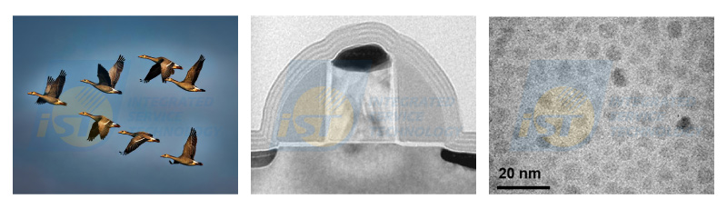
Figure 1: Cases of self-alignment in nature and physics. (a) flying wild geese, (b)Schematic diagram of semiconductor device MOS structure, (c) well aligned nano particles.
K factors of different manufacturer are slightly different. K factors of elements with atomic number larger than 11 are almost same because energies of X-rays emitting from these elements are higher than 1.0 KeV. For elements of C, N, and O, corresponding energies are lower than 0.6 KeV. K factors of these three elements vary from manufacturer to manufacturer due to absorption effect. The difference in K factors will result in large deviation in EDS quantitative analysis. Unfortunately, oxide, nitride, and carbide are all important materials for semiconductors of first, third, and fourth generations.
2. The model for Self-Calibration in TEM/EDS Quantitative Analysis
Materials discussed in this article are divided into two groups according to their morphology. When regions to be analyzed are random distributed, they are the type I material system (material system A), while the type II material system (material system B) are thin-film materials.
(1) Material System A
Supposing x grams of element A and y grams of element B are melted into a single-phase alloy, the weight percent of A and B in this alloy is CA(= [x/(x+y)] x 100%) and CB (= [y/(x+y)] x 100%) , and CA+ CB = 1. When a designed heat treatment is applied to this alloy, the alloy decomposes into (eutectoid) two phases, α and β. Both α and β grains are consisted of elements A and B, but have different compositions with each and the matrix. Figure 2 displays a schematic diagram of a simple model showing the microstructure of this kind of material. Under same (S)TEM operation conditions and same collection time. IAo and IBo stand for intensities of elements A and B of a region including dozens of α grains and β grains. IAα and IBα stand for intensities of elements A and B of the α grain. IAβ and IBβ stand for intensities of elements A and B of the β grain.
![TEM EDS Calibration Supposing x grams of element A and y grams of element B are melted into a single-phase alloy, the weight percent of A and B in this alloy is CA(= [x/(x+y)] x 100%) and CB (= [y/(x+y)] x 100%) , and CA+ CB = 1. When a designed heat treatment is applied to this alloy, the alloy decomposes into (eutectoid) two phases, and . Both and grains are consisted of elements A and B, but have different compositions with each and the matrix. Figure 2 displays a schematic diagram of a simple model showing the microstructure of this kind of material. Under same (S)TEM operation conditions and same collection time. IAo and IBo stand for intensities of elements A and B of a region including dozens of grains and grains. IA and IB stand for intensities of elements A and B of the grain. IA and IB stand for intensities of elements A and B of the grain.](https://www.istgroup.com/en/wp-content/uploads/2025/02/tech_20250318-TEM-EDS-Calibration-02.jpg)
Figure 2:Schematic diagram shows the microstructure of a binary metal material system. (a) as melted alloy, single phase(b) after a designed heat treatment, α and β phases. (Sources:iST)
In this case, the composition of this alloy sample is known, and can be taken to be a standard. Compositions of α phase and β phase can be calculated from some simple equations list below:
CAα = [IAα / IAo] x CA
CBα = [IBα / IBo] x CB
CAβ = [IAβ / IAo] x CA
CBβ = [IBβ / IBo] x CBAuthor had used this method to analyze composition of α phase and β a ternary super alloy for advisor in 1992. The calculated result has only 2 at% difference with the data reported by a paper, which is the only one at that time, of this material system. Both eutectoid materials and high-entropy alloys should be good candidates for this kind of quantitative EDS micro-analysis technique.
(2) Material system B
Figure 3 illustrates a schematic diagram of a typical multi-thin-film material. Many current semiconductor devices have similar configuration. If some layers in this thin film material have one or two elements in common, and one or two layers of thin films are stoichiometric composition, then they can be used to be standards to calibrate compositions of other layers. Firstly, a set of spectrum image is acquired by using STEM/EDS[4], after processed by the built-in EDS program, a line profile is extracted from the processed data. If compositions of thin films are not correct, the proportion of the light element is modified by timing a constant larger than one to meet the stochiometric composition of the compound. Compositions of thin films containing this light element will be changed. An example will be given to prove the feasibility of this method.
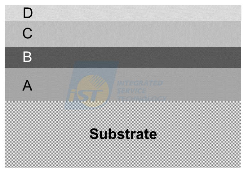
Figure 3:Schematic diagram shows a multi-thin-film materials system
(Sources:iST)3. GaN/GaOx/SiO2 thin films
The example given below was published in IPFA 2022[5] and discussed briefly in iST Classroom (Read more: How to Identify & Analyze Ga2O3?). A further discussion about how to further process results obtained by TEM built-in EDS software. A STEM BF image of a cross-section sample is shown in Figure 4(a). This sample is a GaN device undergoing heat treatment in oxygen rich environment. A layer of SiO2 was then coated upon it by magnetron of sputtering after cooling. Figure 4(a) indicates that two layers of reactants, IA and IB, were formed on the surface of GaN. Figure 4(b) ~ 4(e) are EDS maps of Ga, N, O, and Si respectively. Figure 5(a) is the corresponding STEM HAAD image of Figure 4(a). The yellow dash arrow in the STEM HAAD image marks the trace of EDS line profiles.
Figure 5(b) is the EDS line profiles extracted from the EDS spectrum image along the trace shown in Figure 5(a). EDS analysis shows that reactants IA and IB contains Ga and N only and their composition are very close. The atomic percentage ration of oxygen and gallium of the reactant calculated from a flat region in the EDS line profiles, as marked by the red dotted rectangle in Figure 5(b), is 1.23 to 1. The chemical formula of the reactant, according to this ratio, is Ga5O6 which is not able to be found in web search.
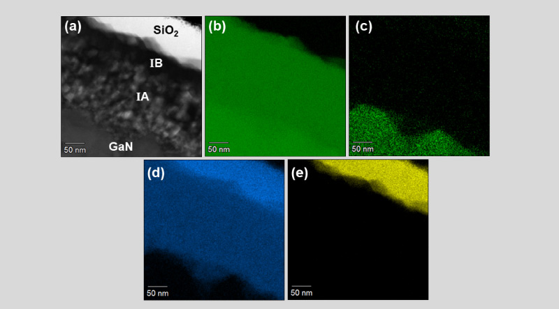
Figure 4: STEM/EDS analysis of reactants on the GaN surface. (a) STEM BF image, (b) Ga map, (c) N map, (d) O map, (e) Si map.
(Sources:Professor Wei-Chih Lai, Department of Photonics, NCKU, 2022)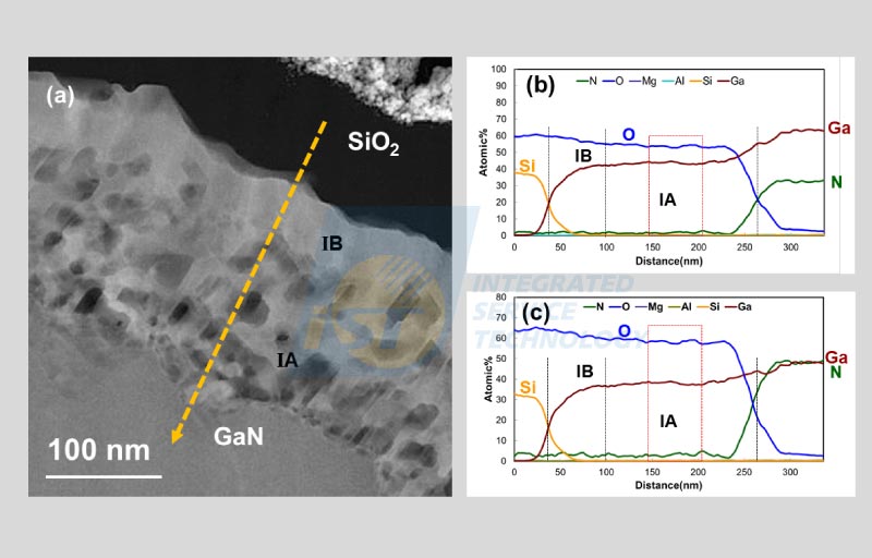
Figure 5: STEM/EDS analysis of reactants on the GaN surface. (a) STEM HAADF image, (b) EDS line profiles calculated by the built-in software, (c) EDS line profiles corrected by self-calibration method.
(Sources:Professor Wei-Chih Lai, Department of Photonics, NCKU, 2022)An article in early iST’s Classroom mentioned that X-rays of N and O were partially absorbed during escaping off the specimen (Read more: TEM EDS Analysis Inaccuracy Caused by Light Element Absorption). Intensities of X-rays of these light elements detected by the EDS detector are usually lower than those generated in the specimen. Checking data at both sides in Figure 5(b) carefully, we found that the atomic percentage of oxygen is not twice as much as silicon at the left side, and the atomic percentage of nitrogen is significantly less than that of gallium at the right side. The built-in EDS software in TEM can process signals detected, but can’t deduce the extent of absorption. So, if we accept these kinds of data without any question, there will be a big mistake in this result.
Now, let us increase the atomic percent of oxygen to be twice of silicon and the atomic percent of nitrogen to be same to that of gallium, then recalculate the atomic percent. The modified results are shown in Figure 5(c). The composition of the reactant deduced from the same region in the line profile discussed early changes to be Ga2O3 which is the most stable phase of gallium oxide [7]. Ga2O3 is claimed to be the semiconductor material of the fourth generation.
In this case, the thin film of unknown composition happens to be located between two layers of stoichiometric compounds, GaN and SiO2. The composition of this unknown thin film can be calculated out more accurately by correcting these two layers of known compositions to be right compositions. This kind of calibration by using neighbor phase of known composition is the key point of the TEM/EDS self-calibration quantitative analysis.
It is the goal of microanalysis to reach accurate TEM/EDS quantitative analysis. Traditional EDS quantitative analysis always needs standard specimens to do calibration. Current EDS standardless quantitative analysis uses K-factors instead of standard specimens. It has been a mainstream technology in TEM/EDS quantitative analysis to employ a set of K-factors, accounting for the relative efficiency of detection of X-rays and using K factor of Si to be 1. However, this method doesn’t take absorption effect into calculation when light elements are involved. When some phases of known composition are introduced into the material containing objects to be analyzed, they can be used to be standards to accurately calibrate compositions of unknown phases. When a TEM specimen contains standards and objects simultaneously, it will make self-calibration EDS quantitative analysis much easier because TEM operation parameters are identical. The key point of self-calibration EDS quantitative analysis is how to make a TEM specimen containing standards as well as objects. Due to this barrier, self-calibration TEM/EDS quantitative analysis can be applied to some material systems only.
Acknowledgments
The sample used is this article was supplied by Professor Wei-Chih Lai, Department of Photonics, National Cheng Kung University. Just acknowledgment here.
References
[1] D. B. Williams and C. B. Carter, in Transmission Electron Microscopy, Chapter 35, (2009).
[2] G. Cliff and G. W. Lorimer, The quantitative analysis of thin specimens, J. Microscopy, 103[2], p.203-207 (1975)
[3] J. H. Paterson, J. N. Chapman, W. A. P. Nicholson, and J. M. Titchmarsh, “Characteristic X-ray production cross-sections for standardless elemental analysis in EDX”, J. Microscopy 154, 1-17 (1989).
[4] Dale E. Newbury and David S. Bright, “Derived Spectra” Software Tools for Detecting Spatial and Spectral Features in Spectrum Images, Scanning vol. 27, 15–22 (2005).
[5] Jong-Shing Bow, Jay Wang, Wei-Chih Lai , Tien-Yu Wang, Syuan-Yu Sie, Sheng-Po Chang, Cheng-Huang Kuo, Jinn-Kong Sheu, Characterization of Oxide Layers on AlGaN Based DUV LEDs by TEM/STEM Analysis, IPFA 2022, 155 (2022).
[6] Jong-Shing Bow, How to Identify & Analyze Ga2O3? iST Classroom.(2022).
[7] T. Oshima, T. Okuno, N. Arai et al., “Vertical sola-blind deep-ultraviolet Schottky photodetectors based on β- Ga2O3 substrates,” Appl. Phy. Express, 1(1):011202 (2008).