Issued Date:2025/1/7A14
Issued By:iST
As the A14 process is set to launch, the semiconductor industry faces unprecedented challenges in analyzing materials at the nanoscale. With high-resolution electron microscopy reaching its limits, Atom Probe Tomography (APT) emerges as a transformative technology. This advanced analytical tool has already been applied to a variety of materials and semiconductor devices. But what exactly is APT, and how are its needle-shaped samples prepared?
A14
The dimensions of semiconductor devices have now been reduced to the nanoscale, with some reaching the atomic scale. Furthermore, the development of heterogeneous integration and three-dimensional devices has significantly increased the challenges faced in high-resolution transmission electron microscopy (HRTEM). As a result, there is a growing need for innovative techniques to address these complexities effectively.
Major wafer manufacturers has announced that process of A14 (14Ǻ) will be rolled out sometime in 2027 ~ 2028. A critical factor in the ongoing chip war is the advancement of process equipment and yield control. The capability of materials characterization techniques, particularly their spatial resolution, has become increasingly significant as semiconductor devices continue to evolve. This article will focus on two key topics: “Atom Probe Tomography (APT) – the latest technique in the academic and research community in Taiwan” and “How to characterize defects within semiconductor devices.”
A14
A14
1. What is Atom Probe Tomography?
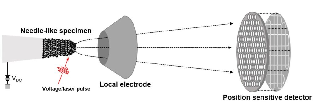
Atom Probe Tomography (APT) is currently one of the most advanced materials characterization techniques. It provides the ability to map the distribution of atoms within a small 3D region with sub-nanometer spatial resolution. Its detection limit reaches approximately 10 ppm within a 20 x 20 x 10 nm³ volume, making it an invaluable tool for precise dimensional and doping concentration control. Recognizing its importance, leading semiconductor companies such as TSMC, Samsung, and Intel have adopted this cutting-edge technique within their operations.
APT works on principles fundamentally different from electron microscopy, which relies on interactions of electron-beam with the specimen. Instead, APT utilizes field evaporation, a process in which atoms on the tip of a needle-shaped sample are ionized and projected onto a position-sensitive detector, to view the atomic arrangement in the sample. So, it bypasses optical diffraction limit. This technique analyzes 3D microstructure of devices or materials, and offers key data for research.
Key Steps in APT Analysis:
- Field Evaporation of Atoms:
The sample is prepared into a needle-like shape with a tip curvature radius must be smaller than 100 nm. By applying high voltage or laser pulses, atoms are evaporated from the tip surface, one by one. - Ion Trajectory and Detection:
Ionized atoms fly toward a position-sensitive detector, which captures their impact positions and time-of-flight. - Mass Spectroscopy:
Time-of-flight data are used to characterize the type of ionized atoms, such as iron or nickel, through mass spectrometry analysis. - 3D Reconstruction:
These collected data are combined to generate a three-dimensional atom map of the material.

(Source: Department of Materials Science and Engineering, NTU)
- Field Evaporation of Atoms:
2. Defects of the Semiconductor Device in Single Data
For R&D and failure analysis of devices, a technique capable of analyzing local compositional variations—such as in thin films, grain boundaries, and junctions—is often essential. While Secondary Ion Mass Spectrometry (SIMS) offers nanoscale depth resolution and a detection limit in the parts-per-million range, it cannot effectively resolve 3D nanoscale structures. TEM can perform compositional analysis using Energy Dispersive Spectroscopy (EDS) and Electron Energy Loss Spectroscopy (EELS), but it faces challenges with 3D nanoscale structures, detection limits, and varying elemental sensitivities. These limitations prevent TEM from providing comprehensive analytical evidence and data.
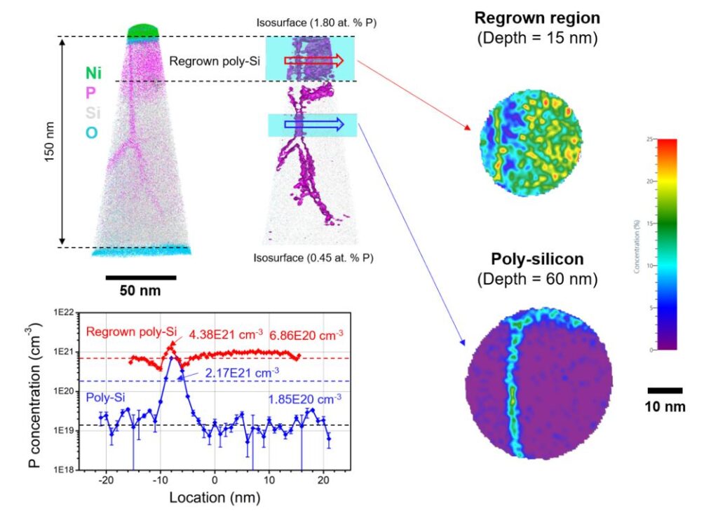
A research team from National Taiwan University (NTU) and the Taiwan Semiconductor Research Institute (TSRI) has investigated doping segregation and diffusion in phosphorus-doped polycrystalline silicon (poly-Si) using APT. They observed a significant drop in carrier concentration in the poly-Si following rapid thermal annealing (RTA). Previously, this reduction in carriers was attributed to incomplete recrystallization or crystal defects. As shown in Figure 1, however, APT analysis revealed that phosphorus atoms segregated at grain boundaries and diffused into the substrate along these boundaries after annealing. The APT data provided 3D distributions of elements, which were further analyzed to generate 2D maps of specified cross-sections and 1D line profiles along designated traces to investigate the segregation phenomenon. The findings of this study highlight that the activation rate of carriers in poly-Si is influenced by the segregation of dopants. Importantly, the segregation of doping elements can be mitigated by optimizing the parameters and methods used during thermal annealing. Once segregation of phosphorus is reduced by optimizing annealing process parameters or methods, the electrical performance, process stability, and device performance can all improved.

Figure 1: APT analysis of rapid thermal annealed P-doped poly-silicon
(Source: Department of Materials Science and Engineering, NTU)Each of these three techniques, APT, TEM, SIMS, has its own advantages and limitations. You can select the most suitable one based on requirements in R&D and characteristics of samples. (If you need a comparison table, please contact the iST representative listed below this article.)
3. How to prepare APT samples?
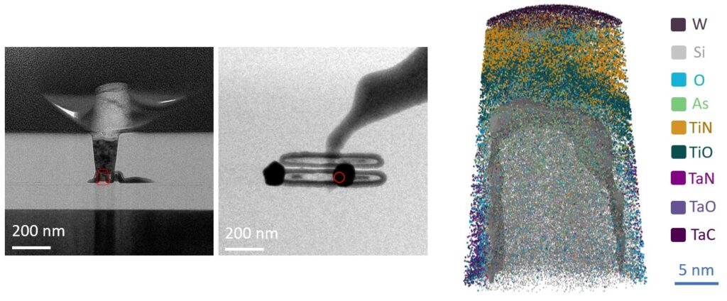
For APT analysis, the sample must be prepared as a tiny tip specimen with a tip radius of curvature smaller than 100 nm. This sharp tip enhances the electric field effect, reducing the potential difference (approximately several thousand volts) required to evaporate and ionize atoms from the surface. Currently, semiconductor device or thin-film samples can only be prepared using Dual Beam Focused Ion Beam (Dual Beam FIB) techniques. iST’s Materials Analysis (MA) lab has collaborated with National Taiwan University to develop a standardized method for preparing tip specimens. These include thin-film samples, MRAM samples, AlGaN optoelectronic devices, FinFET semiconductor devices, and various metals. Figure 2 illustrates a FinFET needle specimen prepared by iST alongside its corresponding APT data. Notably, iST is the first company in Taiwan to be trained and certified by the national APT team to prepare APT tip specimens, establishing a significant milestone in advanced materials analysis.

Figure 2: SEM images of a FinFET needle and the corresponding APT reconstruction map. (Source: Department of Materials Science and Engineering, NTU)
At iST, we are committed to sharing our expertise in materials analysis. If you have any questions or would like to learn more about APT, TEM, or SIMS, please contact our materials analysis lab. We offer tailored guidance to help you select the right analytical tool for your research needs.
For inquiries, please contact Mr. Lin at +886-3-579909 ext. 6166
Email: web_ma@istgroup.com;marketing_tw@istgroup.com
As a VESA-certified laboratory, iST continues to share the latest standards. In a rapidly evolving product landscape, beyond standard certification tests, we leverage our extensive experience to assess customer-provided block diagrams or related data, recommending appropriate test procedures. For non-standard products, iST Signal Integrity Testing Lab can discuss the desired tests with clients’ engineering team to evaluate feasibility and ensure the best assistance and results during the testing process.
For any questions regarding DisplayPort certification, feel free to contact iST Signal Testing Laboratory at +886-2-2792-2890 ext. 2738, Mr. Chris | Email: web_si@istgroup.com;marketing_tw@istgroup.com
Authors of this article:
Prof. Hong-Wei Yen and Dr. Yu-Ren Tseng, Department of Materials Science and Engineering, National Taiwan University