Issued Date:2024/10/09wafer laser dicing
Issued By:iST
Have you encountered inconsistencies or edge chipping with traditional wafer dicing machines when processing hard or brittle materials in semiconductor manufacturing?
As advanced packaging technologies and the complexity of composite materials evolve, have conventional dicing methods proven inadequate, signaling the need for more sophisticated, high-performance solutions?
wafer laser dicing
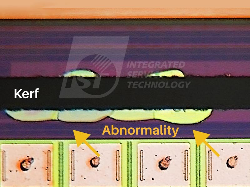
As semiconductor manufacturing becomes increasingly complex and component sizes on wafers continue to shrink, advanced processes push the boundaries of technical limitations, while material technology rapidly evolves. The rise of wide bandgap semiconductors and breakthroughs in advanced packaging have opened new frontiers in the semiconductor industry. However, traditional physical dicing methods, such as blade cutting used for silicon wafer packaging, are struggling to meet these new challenges. This is particularly true when handling hard and brittle materials, such as low dielectric wafers, SiC, and AlN, where issues like wafer edge peeling and chipping frequently arise, negatively impacting yield and performance. In many applications, even minor structural damage or surface defects can lead to component failure, which is critical in advanced semiconductor devices.
Laser dicing has been applied to wafer cutting for more than a decade, but it’s recently gaining renewed attention due to the emergence of new applications. Unlike traditional mechanical cutting, UV laser dicing uses high-energy laser beams to perform non-contact cutting, sublimation materials to achieve separation. This method not only reduces mechanical stress on the wafer but also enables precision processing of complex materials without compromising product performance. As semiconductor processes continue to advance, laser dicing has become a critical tool in wafer cutting technology.
wafer laser dicing
wafer laser dicing
1. Differences Between Laser Dicing and Traditional Dicing
Traditional wafer dicing uses physical blades to cut materials through mechanical contact, but this method has notable limitations in precision and flexibility. It’s particularly challenging when dealing with newer or unfamiliar materials, which makes choosing the right blade and optimizing settings difficult. In contrast, laser dicing utilizes high-energy lasers for non-contact cutting, sublimation the material with thermal energy. This method allows for fine control over the cutting process, offering more flexibility by adjusting laser optics and energy levels.
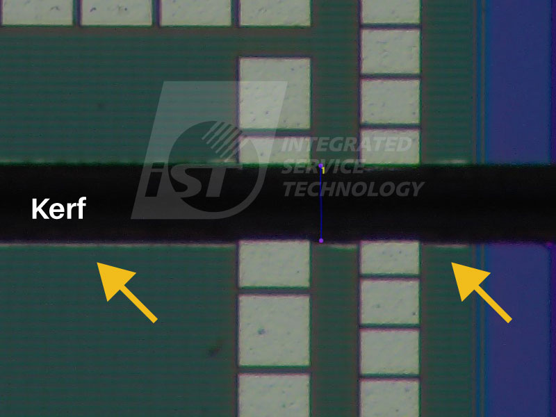
One major drawback of traditional dicing is the mechanical stress it places on the wafer, which increases the risk of cracks and edge damage. Laser dicing eliminates this issue by using non-contact cutting, which removes the risk of mechanical stress. Additionally, high-frequency laser systems minimize thermal stress, reducing the likelihood of defects after cutting.
Traditional methods also struggle with the advanced materials used in today’s semiconductor manufacturing. The cutting speed is often limited by the material’s properties, which affects both efficiency and quality. Laser dicing offers significant advantages here, providing faster and more consistent cuts, which are ideal for large-scale production. The non-contact nature of laser cutting also reduces material loss, resulting in better yield and overall performance.
Comparison Traditional Dicing Laser Dicing Cutting Method Uses physical blades for contact-based cutting Relies on high-frequency, high-energy laser beams for non-contact cutting Precision and Flexibility Limited precision, struggles with small structures and complex patterns High precision, ideal for narrow dicing lanes and intricate components Mechanical Stress Physical contact generates stress, increasing the risk of cracking Non-contact, reduces mechanical stress, minimizing damage risk Material Compatibility Poor performance with brittle materials, prone to edge chipping Excellent for complex materials, highly flexible in various cutting processes Processing Speed Slower, efficiency affected by material properties Fast and consistent, suited for high-performance mass production Material Loss Significant material loss due to physical contact Minimal material loss with non-contact technology, improving yield 2. How Can iST and ProPowertek Assist?
To address the increasing demand for precision and efficiency in the semiconductor industry, we have introduced advanced laser dicing equipment, which is deployed across two of our companies—iST and ProPowertek—to offer enhanced cutting services tailored to different stages of the customer’s production process.
- iST: At the product development stage, iST focuses on providing engineering sample fabrication services. With laser dicing technology, iST can deliver highly accurate samples for a wide range of new materials and structures, aiding in subsequent reliability testing and product development analysis. This technology significantly reduces defect rates during sample fabrication, improving both precision and efficiency in the R&D phase.
- ProPowertek: In the mass production stage, ProPowertek specializes in wafer thinning, testing, and dicing services. Laser dicing not only reduces the risk of chipping after wafer thinning but is also a powerful solution for cutting third-generation semiconductors. In addition to providing superior cutting quality, this technology boosts overall production efficiency, helping customers achieve high-quality, stable output during mass production. This is critical for maintaining yield and reliability in semiconductor manufacturing.
Our solutions are designed to help clients achieve more efficient product development and mass production at every stage, leveraging powerful tools and accumulated expertise to enhance overall competitiveness. If you would like to further understand the details, please feel free to contact us:
- iST │ +886-3-579-9909 ext. 6861 │ Mr. Chen │ ist_assy@istgroup.com
- ProPowertek │ +886-3-579-9909 ext. 5888 │ Mr. Yu │ contact@propowertek.com


