Issued Date:2024/2/22 GaN dislocation
Issued By:iST

The wide band gap semiconductors represented by Gallium Nitride (GaN), tends to generate a significant number of dislocation defects due to process-related factors. The density and types of dislocations play a crucial role in influencing the functionality of semiconductor devices. Although the industry can detect dislocation density with other instruments, only TEM can characterize dislocation types. How does TEM achieve this?
GaN dislocation
The current trend in the wide band gap semiconductors focuses on GaN (Gallium Nitride) and SiC (Silicon Carbide). These materials are prominent in high-frequency communication devices and power semiconductor components. Historically constrained by factors such as limited material availability and high costs, these materials were primarily applied in defense and aerospace. In recent years, with advancements in semiconductor technology and cost reduction, their usage has gradually expanded to include industrial, automotive, and consumer electronics industries. GaN dislocation
GaN, in particular, stands out among semiconductor materials due to its resistance to high voltage and temperature, low resistance, excellent electrical and thermal conductivity, small size, and low energy consumption. As the world moves towards achieving net-zero emissions, market research firm Yole predicts that the market value of GaN will grow from $184 million in 2022 to $2.04 billion in 2028. However, a significant drawback of GaN is the high density of dislocation crystal defects within its single crystal compared to other semiconductor materials. Both the density and type of dislocations in the single crystal of GaN are crucial factors that influence the likelihood of leakage current in future devices, potentially leading to functional abnormalities.
Currently, Transmission Electron Microscopy (TEM) BF (Bright Field) images of two beam conditions is currently the only one micro-nano material analysis technique that can characterize kind of dislocations. This article will briefly introduce a method that characterizes types of dislocations in GaN epitaxy.
Some basic concepts of dislocations and TEM techniques for analyzing dislocations will be introduced first to help readers understand how to use TEM techniques to analyze dislocations in GaN crystals, then go to the topic of characterization of dislocations in GaN epitaxy.
GaN dislocation
GaN dislocation
1. Characterization of Dislocations in GaN Epitaxy
In the field of materials of science and engineering, solid state inorganic materials can be divided into two categories: crystal and amorphous. The main difference of these two is the arrangement of atoms. There is no order, or very short-range order (smaller than 2 nm), in amorphous solid materials. The typical amorphous material observed in daily life is glass. That’s why amorphous phase is also named glass phase. The arrangement of atoms in crystals is long term order in three dimensions. In our daily life, materials, such as gold, silver, copper, iron, and aluminum, are crystals. Crystalline materials are divided into single crystal and polycrystal materials. Metals mentioned before are polycrystal materials, and Si wafers are the representative of single crystal materials. Single crystals are the fundamental for the semiconductor industry. From the first category of semiconductor to the third category of semiconductor devices [1], all must use single crystal substrates to manufacture semiconductor components.
Silicon and Germanium are semiconductor materials of the first category. Defects density in these single crystals is very low, only a few of vacancies, while dislocations are almost zero. GaAs is the typical semiconductor material of the second category, and its wafer quality is as good as that of silicon wafers. GaN is one of semiconductor materials of the third category. It is hard to grow GaN single crystal ingots. So, GaN semiconductor devices are manufactured on GaN epitaxy on several kinds of substrates [2]. Most GaN epitaxy are grown on (0001) sapphire substrates with [-1010]GaN // [1-2 1 0]sap, [1 -2 1 0]GaN // [10 -10]sap epitaxial relationship. D-spacings of (10 -10) sap and (1-2 10) sap are 0.1374 nm and 0.2379 nm separately, and d-spacings of (1-2 10) GaN and (-1010) GaN are 0.1593 nm and 0.2759 nm. The lattice mismatch between these two crystals is about 16%. Dislocations are generated at the interface to relax the strain between crystals and extend into GaN epitaxy [3]. It has been an important research topic to explore dislocations, density and types, in the GaN/sapphire material system.
2. Types of Dislocation and Burger’s Vector
A schematic diagram of a perfect crystal is shown in Figure 1. There is no misaligned lattice (or atom) in this model. If we start from an arbitrary lattice point (atom) on a random cross section of this crystal, then move m units to the right, and move n units down, and m units to the left, finally n units upward. We go back to the starting lattice point. The path forms a close loop, as shown in Figure 2(a). If there is a row of misaligned atoms inside the loop and perpendicular to the section, the end point of the path will not coincide with the start point, as shown in Figure 2(b). An extra displacement has to be added to go back to the start point. This kind of misaligned atoms is named edge dislocation, since it looks like a sharp blade being inserted in the lattice. The displacement from the end point to the start point is defined to be Burger’s vector [4, 5] of this dislocation. The dislocation line of an edge dislocation is perpendicular to its Burger’s vector. Figure 2(c) displays other kind of dislocation, the dislocation line is a boundary of moved and unmoved lattice. This dislocation line is parallel to its Burger’s vector. This type of dislocation is named to be screw dislocation, since it goes forward one step after moving along the loop, as a screw does.
Figure 1: A schematic diagram of a perfect crystal. All lattices (or atoms) are well aligned. (Source: iST)
![GaN dislocation The path forms a close loop, as shown in Figure 2(a). If there is a row of misaligned atoms inside the loop and perpendicular to the section, the end point of the path will not coincide with the start point, as shown in Figure 2(b). An extra displacement has to be added to go back to the start point. This kind of misaligned atoms is named edge dislocation, since it looks like a sharp blade being inserted in the lattice. The displacement from the end point to the start point is defined to be Burger’s vector [4, 5] of this dislocation. The dislocation line of an edge dislocation is perpendicular to its Burger’s vector. Figure 2(c) displays other kind of dislocation, the dislocation line is a boundary of moved and unmoved lattice. This dislocation line is parallel to its Burger’s vector. This type of dislocation is named to be screw dislocation, since it goes forward one step after moving along the loop, as a screw does.](https://www.istgroup.com/en/wp-content/uploads/2024/01/tech_20240222-02-Gan.jpg)
Figure 2: A schematic diagram of a cross section of a crystal. (a) a close loop on the section of a perfect crystal, (b) an open loop on the section with an edge dislocation, (c) an open loop on the section with a screw dislocation. b is the Burger’s vector. (Source: iST)
The extra row of atoms in the edge dislocation will push atoms at both sides, which induce a compressive stress field formed among these atoms. The distance of atoms right below this dislocation increase, this makes these atoms pull each to back to their original lattice points. Thus, a tensile stress field is induced at this location. Both these two stress fields are parallel to the Burger’s vector and perpendicular to the dislocation line, as shown in Figure 3(a). For a screw dislocation, the stress making the displacement is parallel to the Burger’s vector and the dislocation line, as shown in Figure 3(b). In Figure 3, the bold letter R represents for the direction of stress. Lattices around the dislocation are distorted due to the stress around. This local distortion changes the angles between the incident electron beam and lattice planes, as shown in Figure 4. The diffraction conditions of these lattice planes are also changed, and this result in an image contrast between lattice planes right around the dislocation and lattice planes a little away from the dislocation and with no distortion. This contrast caused by the difference in diffraction condition makes the dislocation visible. This kind of TEM image contrast is called diffraction contrast since the change in image brightness is caused by the change in diffraction condition. The diffraction condition of undistorted lattice planes and distorted lattice planes change keeps changing during specimen tilting in TEM analysis. At some specified diffraction condition, the different in brightness of all lattice planes is negligible, and the dislocation is invisible under such diffraction condition [6]. This diffraction condition is very important in analyzing dislocations by using TEMs. It will be discussed in the following paragraph.
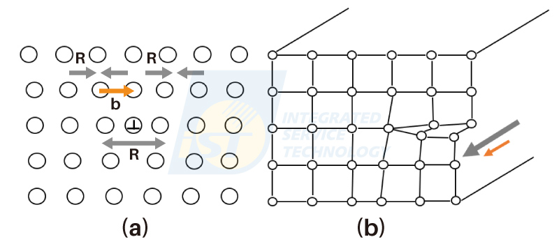
Figure 3: Schematic diagrams show models of dislocation and stress field. (a) the stress field is parallel to Burger’s vector and perpendicular to the dislocation line for an edge dislocation, (b) the stress field is parallel to Burger’s vector and the dislocation line for a screw dislocation. (Source: iST)
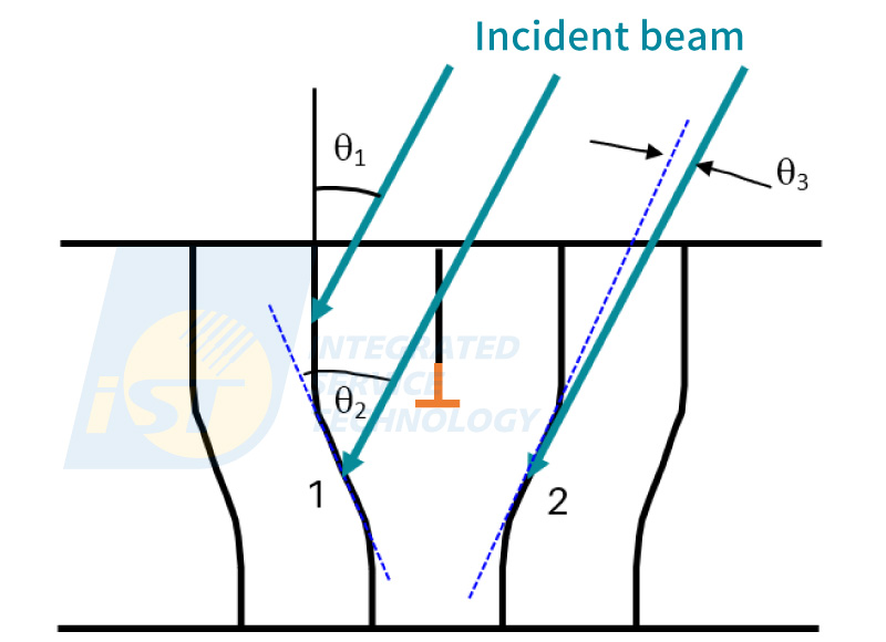
Figure 4: A schematic diagram shows changes in angles between the incident electron beam and distorted lattice planes around the dislocation. θ1is the angle between the incident electron beam and non-distorted lattice planes, θ2 and θ3 are angles between the incident electron beam and distorted lattice planes. (Source: iST)
3. Two Beam Condition and Invisibility of Dislocations
There are three main types of diffraction conditions to analyze crystalline materials. They are exact zone condition, two beam condition, and kinematic condition [4 ~ 6], as shown in Figure 5. Since the transmitted beam exists in all electron diffraction patterns, two beam condition means only one diffraction spot left in the electron diffraction pattern. This special diffraction condition is used to analyze crystal defects. The diffraction condition is simplified to be only one operating vector (g vector) valid. This makes the elucidation of image contrast much easy.
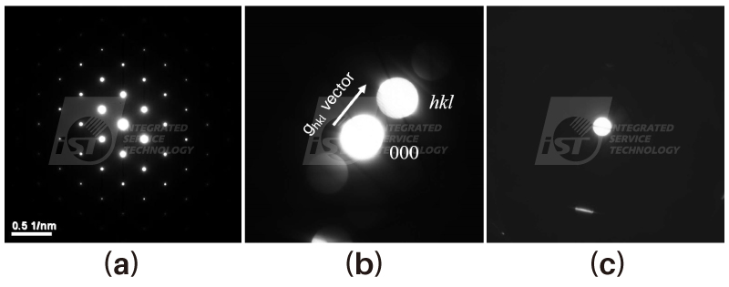
Figure 5: Three typical SADPs (Selected Area Diffraction Patterns) of single crystals. (a) exact zone condition, (b) two beam condition, (c) kinematic condition. (Source: iST)
The dot product of g vector and R (crystal displacement) is zero when these two vectors are perpendicular to each other. The brightness of dislocations is same to that of matrix around, since the diffraction condition is almost same, so the dislocation is invisible at this two-beam condition, as shown in Figure 6. The dislocation marked by a white arrow (Figure 6(a)) is invisible in Figure 6(b)[7].
![GaN dislocation The dot product of g vector and R (crystal displacement) is zero when these two vectors are perpendicular to each other. The brightness of dislocations is same to that of matrix around, since the diffraction condition is almost same, so the dislocation is invisible at this two-beam condition, as shown in Figure 6. The dislocation marked by a white arrow (Figure 6(a)) is invisible in Figure 6(b)[7].](https://www.istgroup.com/en/wp-content/uploads/2024/01/tech_20240222-06-Gan.jpg)
Figure 6: TEM BF (Bright Field) image of Si substrate under two beam conditions. (a) a dislocation is marked by a white arrow, (b) the marked dislocation disappeared. Corresponding CBED (Convergent Beam Electron Diffraction) patterns are shown below BF images. [7] (Source: iST)
4. Analysis of Dislocations in GaN Grown on Sapphire Substrate
One pair of TEM BF (Bright Field) images of GaN/sapphire taken under a set of two beam conditions are shown in Figure 7. The operating g vector in Figure 7(a) is [1 -100], and that in Figure 7(b) is [000 -1], these two g vectors are perpendicular to each other. One pair of black and white arrows shown in these two BF images are used to mark the corresponding positions in these two images. Those dislocations labelled “E” in Figure 7(a) run along [0001] and are all invisible in Figure 7(b), this indicates that the strain fields of these dislocation are all perpendicular to [0001]. We thus deduce that these dislocations are edge dislocations according to the relationship of dislocations and strain field shown in Figure 3.
![GaN dislocation One pair of TEM BF (Bright Field) images of GaN/sapphire taken under a set of two beam conditions are shown in Figure 7. The operating g vector in Figure 7(a) is [1 -100], and that in Figure 7(b) is [000 -1], these two g vectors are perpendicular to each other. One pair of black and white arrows shown in these two BF images are used to mark the corresponding positions in these two images. Those dislocations labelled “E” in Figure 7(a) run along [0001] and are all invisible in Figure 7(b), this indicates that the strain fields of these dislocation are all perpendicular to [0001]. We thus deduce that these dislocations are edge dislocations according to the relationship of dislocations and strain field shown in Figure 3.](https://www.istgroup.com/en/wp-content/uploads/2024/01/tech_20240222-07-Gan.jpg)
Figure 7: TEM BF images of GaN/sapphire under two beam conditions. (a) g vector [1 -1 00], (b) g vector [000 -1]. Corresponding SADP patterns are inserted at lower right corners of TEM BF images.
As the applications of GaN continue to diversify, comprehensive control over the dislocation quality of GaN is crucial for the subsequent functionality of devices. While there are instruments on the market capable of scanning dislocation density on a large scale, the TEM dual-beam diffraction imaging is currently the only material analysis tool that can characterize the type of dislocations in GaN. This article introduces the analysis technique briefly. It will take times to photo enough TEM BF images of two beam conditions to meet the statistical requirements and to deduce the causal relationship between dislocation types and density and device quality, continuous accumulation of TEM image capture and analysis work is necessary. Despite being time-consuming, this is a vital forward-looking research endeavor for a profound understanding of the properties and influencing factors of GaN single crystals. GaN dislocation
iST’s Material Analysis Laboratory has extensive experience and successful cases in the semiconductor process and advanced packaging fields. In this article, we share this knowledge with our long-time supporters. If you have related needs or would like to further understand this knowledge, please feel free to contact marketing_tw@istgroup.com.
References:
[1] Julissa Green, “Detailed Introduction to Three Generations of Semiconductor Materials”, 2023. https://www.sputtertargets.net/blog/introduction-to-the-generations-of-semiconductors.html
[2] Shuji Nakamura, Stephen J. Pearton, and Gerhard Fasol, in “The Blue Laser Diode, The Complete Story”, chapter 4, published Springer-Verlag, Berlin, Heidleberg, New York, 2000. ISBN: 3-540-66505-6
[3] Fernando A. Ponce, “Microstructure of Epitaxial III-V Nitride Thin Films” in “GaN and Related Materials”, edited by Stephen J. Pearton, published by Gordon and Breach Science Publishers, USA, 1997. ISBN: 90-5699-517-0
[4] 鮑忠興和劉思謙, 近代穿透式電子顯微鏡實務, 第二版, 台中: 滄海書局, 2012. ISBN: 978-986-5937-22-5.
[5] G. Thomas and M. J. Goringe, Transmission Electron Microscopy of Materials, John Wiley & Sons, Inc., New York (1979). ISBN: 0-471-122440-0
[6] David B. Williams and C. Barry Carter, in Transmission Electron Microscopy, Microscopy, part 2, Plenum Press, New York (2007). ISBN: 0-471-122440-0
[7] J. S. Bow and Speed Yu, “Depth Measurement of Dislocations in Si Substrate by Stereo TEM,” Proc. ISTFA, 233-234 (2005).