Issued Date:2023/4/25 TEM sample preparation
Issued By:iST

The same water that can carry a boat can also capsize it.
Inertia thinking may enable you to become more proficient, but it may also cause you to overlook critical information in a TEM sample!
In this article, Uncle Bow uses his own experiences to demonstrate how human habitual thinking can misplace the results of TEM material analysis.
TEM sample preparation
In physics, an object that is not subjected to external forces will continue to move at a constant speed along a straight line, which is known as inertia. In our daily routine traffic, after having driven from place A to place B daily for years, most people become accustomed to driving along one or two routes. Occasionally, we may forget to make a turn at the right intersection when we want to buy something at the middle way, place C. I refer to this mistake as “being lost in inertia” that happens in daily life from time to time for many people. Most of them are harmless. However, when it happens in engineering cases and/or business cases, it can result in some degree of damage. The loss may be only a few of manpower and material resources, or may be a huge damage to the enterprise.
TEM sample preparation
TEM sample preparation
Case 1: Inertia Thinking Leads to Endless Testing Loops and Almost Delays the Delivery Date?
More than twenty years ago, while working at the Materials Research Laboratory (MRL) at the Industrial Technology Research Institute (ITRI), I encountered a case of yield issues in a semiconductor device. Two sets of epi Si wafers underwent the same process, but Set A had a yield of less than 50%, while Set B had a yield of over 95%. My task was to identify the defects in the epi layer. To do so, I used TEM to analyze the cross-sectional structure of the samples.
On the first day, I prepared a TEM specimen of Set A and found several nanoscale voids at the interface of the epi layer and Si substrate. On the second day, I prepared a TEM specimen of Set B, but nothing except Si substrate was observed. I suspected that the grinding and polishing were done in the wrong place, so I made a second TEM specimen of Set B on the third day.
Unfortunately, there was still only one single crystal observed in TEM. The interface of epi Si layer and the Si substrate as observed in set B was not found.
The third TEM specimen of sample B was prepared and checked in the TEM on the fourth day, which was one day before the deadline. It was around 11:00pm, and there was still no solid data on sample B to deliver. I walked out of the TEM laboratory to take a break and pondered what could have gone wrong with the TEM sample preparation for sample B, as well as how to ask the customer for a one- or two-day extension. While meditating, something came to my mind – nothing was wrong. The interface between the homogeneous epitaxial layer and the substrate is invisible when the epitaxial layer is well-grown.
I had been trapped in the inertia of my previous knowledge from analyzing heterogeneous epitaxial layers and the result of sample A for all these days. From sample A, I found out that the thickness of the epi layer was 50 nm. Therefore, all I needed to do was to ensure that the surface of sample B was flat and undamaged. Then, I drew a straight line parallel to the surface at a depth of 50 nm from the surface of the sample and extended it to cover the entire TEM analysis area. If no defects were found near this line, it could be concluded that there were no defects between the epi layer and the Si substrate in sample B.
Mid-break: Have You Also Fallen into the Trap of Inertia Like the Protagonist?
It’s easy to fall into the trap of inertia in our everyday lives, whether it’s in our relationships or our work. A short joke about lost in inertia just came to my mind.
A young couple was strolling in the park when a mosquito accidentally flew into the young lady’s eye.
The young man helped to blow the mosquito off her eye and gently said, “Your eyes are so big!”
The young lady smiled with tears in her eyes.As they continued walking and talking, a mosquito flew into the lady’s mouth while she was speaking.
The young man helped to wipe her saliva and gently said, “Your mouth is so big!”
Their happy time ended.Case 2: Can't We Just Follow the Usual Routine? The Slight Difference in Sample Preparation Leads to Completely Different Results?
Currently, TEM analyses of silicon-based semiconductor devices are typically divided into two main steps: FIB sample preparation and TEM analysis. Since most Si semiconductor devices are made on [001] Si wafers and transistor patterns are aligned along {110} directions, FIB engineers usually cut chips along one of the {110} directions in the first step. In the second step, TEM engineers typically tilt the specimen to the [110] exact zone to align with the electron beam before proceeding with the analysis.
[001], {110}, [110], etc. are Miller indices, which are used to represent crystal directions and crystal planes in crystallography. They are a notation system that is used to determine the arrangement of atoms or ions in a solid.
Figure 1(a) shows a FIB SE image where the yellow arrow points to a location where metal 1 (M1) and a tungsten plug (W) are very close to each other. However, due to the resolution limit of FIB, it is difficult to determine whether they are in contact or not. Therefore, a cross-sectional TEM specimen is required for further TEM analysis. In this non-routine case, the TEM specimen should be cut as indicated by the dashed-line rectangle in Figure 1(b). However, following the inertia thinking, the TEM specimen was cut along the [110] direction, as shown by the dashed-line rectangle in Figure 1(c) for routine cases.
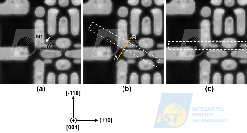
Figure 1:FIB secondary electron image. (a) The yellow arrow points to the area where metal 1 (M1) and tungsten plug (W) are very close; (b) the dashed rectangle
represents the ideal TEM specimen shape; (c) the dashed rectangle represents the
actual TEM specimen shape.If the TEM engineer had followed the conventional method in this case, they would have tilted the specimen to the [110] exact zone condition and taken pictures, as shown in Figure 2(a). The conclusion drawn from this image would have been that the waist of metal 1 had touched the tungsten plug. However, if the specimen had been tilted to a certain degree and viewed nearly along the yellow dotted line AB in Figure 1(a), it would have been found that there was a gap of several nanometers between the waist of metal 1 and the tungsten plug, as shown in Figure 2(b) by tilting the specimen correctly. The information obtained from Figures 2(a) and 2(b) would have led to significantly different design or process adjustments.
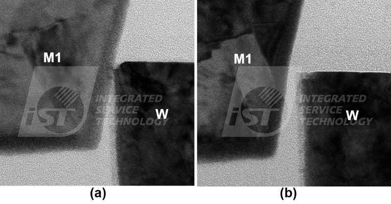
Figure 2:Cross-section TEM bright-field images. (a) TEM bright-field image taken along the positive [110] axis of the silicon substrate, showing that the waist of metal 1 (M1) is in contact with the tungsten plug (W); (b) TEM bright-field image taken after tilting the specimen by more than 20 degrees along the [001] axis of the silicon substrate, showing that the waist of metal 1 and the tungsten plug are not in contact.
Inertia thinking can help us become proficient, but for non-routine cases, standardized inertial operations only yield a large number of neatly arranged images and several sets of color composition maps. Useful information of materials is still trapped inside the specimen and the powerful capability of TEM was not fully used.
This article is the inaugural publication from the Uncle Bow’s Corner series presented by iST Materials Lecture. Dr. Bow explores the topic of inertia thinking, a common phenomenon that can lead to challenges in material analysis using TEM. Have you ever found yourself trapped in this way of thinking? Hopefully, this article can help you break out of it and achieve breakthroughs in both your personal and professional life.
This is to share knowledge and experiences of iST with you. Should there be any inquiry or if you would like to know more about the aforementioned techniques, just email us at marketing_tw@istgroup.com。