Issued Date:2023/1/10Ga2o3, Ga2O3,
Issued By:iST
How to Identify & Analyze Ga2O3?
Because of its outstanding optical properties and small size, AlGaN-based deep ultraviolet (DUV) light-emitting diodes (LEDs) are replacing conventional DUV light sources, such as mercury and xenon lamps[1-3]. Current light output efficiency of AlGaN-based DUV LEDs can be enhanced by modifying epitaxy techniques to improve the quality of AlGaN[4, 5] . One method proposed by Lai et al. [6] is to introduce epitaxial gallium oxide layers on the sidewall of epitaxial layers of GaN and AlGaN.
The purpose of this iST classroom, is to show how to use TEM techniques to characterize the morphology, crystal structure, and composition of these gallium oxides.
Ga2o3
Ga2O3 has an ultra-wide bandgap (4.5 – 4.9 eV). This characteristics makes it be the fourth generation semiconductor which has higher breakdown voltage and critical electric field than those of the third generation semiconductor (III-V compounds), such as SiC and GaN.
I. Configuration of AlGaN-based DUV LEDs
The cross-section structure of AlGaN-based DUV LEDs manufactured by metal-organic chemical vapor deposition (MOCVD) is illustrated in Figure 1a. An aluminum nitride (AlN) layer working as a buffer layer to reduce dislocation density in following AlGaN layers was grown on a sapphire substrate, then two layers of AlGaN with different Al concentrations, multiple quantum well (MQW), electron-blocking layer (EBL), and finally a GaN layer.
This thin film structure was then ICP etched by lithography to form a mesa structure on the top, as shown in Figure 1b. Oxide layers formed on both the top GaN layer and side walls of GaN layer and AlGaN layer after thermal annealing in high temperature with oxygen rich atmosphere. Finally, A layer of high purity SiO2 of 100 nm thick was deposited on the mesa of unannealed and annealed samples by magnetron sputtering [7], as illustrated in figure 1c.
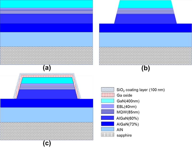
Figure 1:Schematical diagram of cross-section structure of AlGaN-based DUV LEDs. (a)diode as grown by MOCVD, (b)after ICP etched, (c)after thermal oxidation and SiO2 coating. [7]
II. Analyzing product phases by TEM images and electron diffraction
Cross-section TEM (X-TEM) specimens of AlGaN-based diodes of unannealed and annealed were made by focus ion beam (FIB) on selected positions, they were then analyzed by TEM/STEM, image and diffraction, to characterize those oxides formed on the surface of GaN and side-walls of GaN and AlGaN during high temperature annealing.
Two TEM BF images of low-and-medium magnification in figure 2 show the cross-section structure of unannealed and 900℃/20 min annealed AlGaN DUV LEDS respectively. Three new phases, marked 1, 2, and 3, on the surface and the side-wall of the GaN layer and the side-wall of the AlGaN layer were found after comparing these two BF images carefully.
A pair of STEM BF image and ADF image of the 900℃/20 min annealed AlGaN DUV LEDS are shown in figure 3. From the TEM images and STEM images in figure 2 and figure 3, we find that the best TEM imaging technique for this material system is the STEM ADF image.
This can be further confirmed by two sets of STEM images of high magnification in figure 4. STEM ADF images give better contrast to distinguish those three phases. The characteristic image contrast of each phase tells that phase 1 and phase 3 may be polycrystal materials with grains of nano size, and phase 2 may be a single crystal.
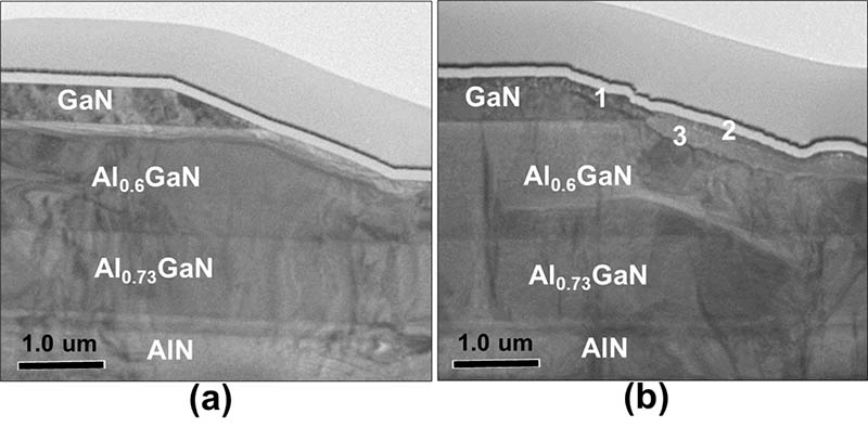
Figure 2:TEM BF images of AlGaN-based DUV LEDs. (a)before thermal annealing, (c) 900℃/20min annealed. [8]
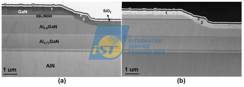
Figure 3:Cross-section images of 900℃/20min annealed AlGaN-based DUV LEDs. (a)TEM BF image, (b) STEM ADF image.
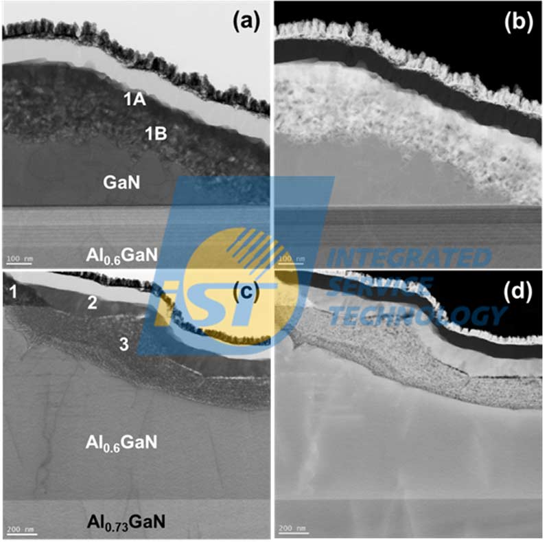
Figure 4:Two sets of high-and-medium magnification STEM images of 900℃/20min annealed AlGaN-based DUV LEDs. (a) and (b) STEM BF image and STEM ADF image of GaN layer with oxide layer respectively, (c) and (d) STEM BF image and STEM ADF image of AlGaN layer with oxide layer respectively.
Figure 5 shows a low magnification STEM BF image and a set of selected area diffraction patterns (SADPs). These SADPs are corresponding to GaN layer, AlGaN layer, and three products (figure 5a). Both GaN and AlGaN are epitaxial layers, corresponding SADPs indicate the view direction is along [1 1 -2 0] zone axis in this TEM analysis. All these three SADPs of oxides are from one zone axis only and not enough to be solved completely at present. However, they are all spot patterns of single array. This type of SADPs indicates that three analyzed areas are all single crystals. These results are somehow contradictory with those results from TEM/STEM image data shown in figure 3 and figure 4.
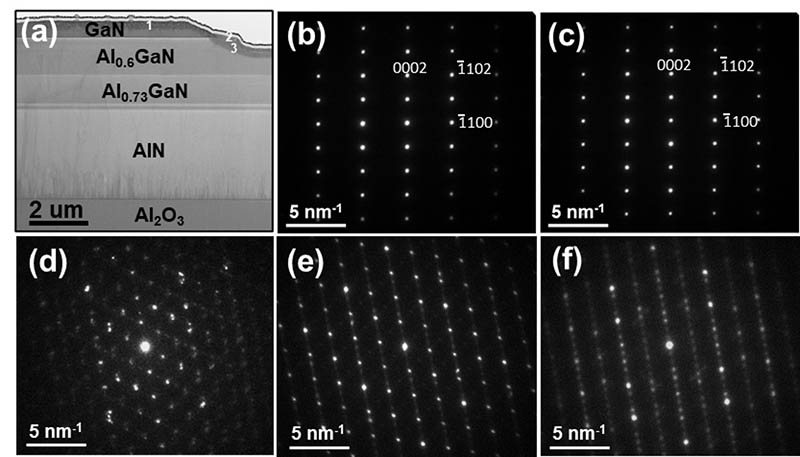
Figure 5: STEM image and SADPs of 900℃/20min annealed AlGaN-based DUV LEDs. (a)low magnification STEM BF image, (b)SADP of GaN layer, (c)SADP of AlGaN layer, (d) SADP of product 1, (e)SADP of product 2, (f)SADP of product 3.
(Courtesy by Dr. Lai)To solve this contradiction, we checked each new phase using its TEM images, STEM ADF image, and SADP, back and forth, and made sure that all these three products were single crystals finally. Black and white image contrast in product 1 and product 3 are atomic number contrast rather than diffraction contrast which is dominant in samples of poly crystals.
We can identify phase 1 and phase 3 to be porous structure definitely by higher magnification STEM ADF images, as shown in figure 6. Dark areas (bright areas in BF image) in these two products are pores. Those pores in phase 1 are obviously larger than those in phase 3. Phase 2 is a dense single crystal with some big pores inside, one of them is pointed by a white arrow in figure 6. The mechanism of forming homogeneously distributed nano pores in phase 1 and phase 3 is considered to be that the diffusion rate of oxygen and gallium atoms is higher than the stacking rate of atoms to crystals in high temperature annealing.
Generally, we need SADPs of several zone axes to solve the crystal structure. It is hard to identify the product phase by using a single SADP to characterize the new phase definitely. However, the simulated β-Ga2O3 [0 1 0] SADP is very similar to SADPs shown in figure 5d, 5e, and 5f. We, thus, infer that these products may be β-Ga2O3 and β-(AlxGa1-x)2O3 on GaN layer and AlGaN layer correspondingly. β-Ga2O3 is a monoclinic crystal, and this makes the analysis work of its SADP complicated and hard.
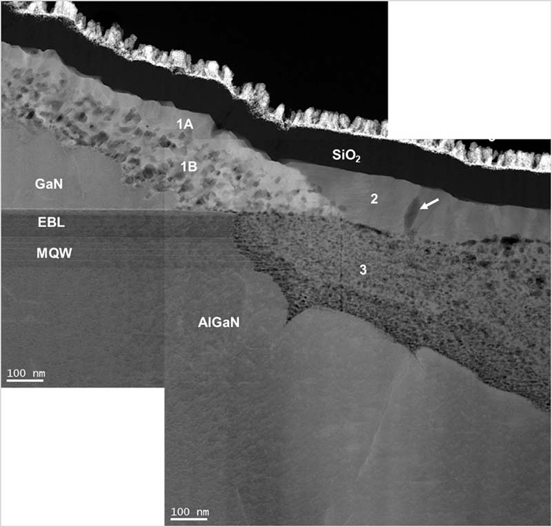
Figure 6:High magnification STEM ADF image shows the morphology of three product phases on GaN and AlGaN layers. [8]
III. STEM/EDS analysis – self-calibration quantitative analysis
Elemental maps of GaN and the product on it, shown in figure 7, are derived by STEM/EDS spectrum image technology. These elemental maps indicate that there are only oxygen and gallium in the product phase. This indicates that the product analyzed is a gallium oxide. The variation in concentration is extracted along the trace indicated by the light blue arrow in figure 8a.
Concentration of elements in line profiles shown in figure 8b is quantitatively calculated by the built-in EDS program using K factors stored in database [9-11]. This kind of quantitative analysis is named to be standardless quantitative analysis which has been widely accepted by journals of science and engineering.
The concentration ratio of O/Ga of oxide 1B is derived from a flat region in the 1B region, indicated in figure 8b, is 1.23. This result indicates the composition of this oxide phase is Ga5O6. This composition is calculated by the built-in EDS program which used X-ray signals emitting from the specimen and being detected by the EDS detector and K factors stored in the database.
However, there is no gallium oxide with composition Ga5O6 reported in literature.
Absorption effect is usually neglected in TEM/EDS analyses which use thin foils to be specimens. However, we found that the absorption effect is still significant and results in large error without awareness when light elements, such as C, N, and O, are included. Checking figure 8b carefully, we find that the ratio of O to Si is much smaller than 2 (left side), and the ratio of N to Ga is obviously smaller than 1 (right side). EDS line profiles in figure 8b are then calibrated by taking stoichiometric compounds of SiO2 and GaN. The calibrated EDS line profiles are then modified as shown in figure 8c. The ratio of O to Ga of the oxide 1B then changes to be 1.53, it means that the gallium oxide is Ga2O3, as reported by Oshima et.al. [12].In TEM(STEM)/EDS analysis, the EDS line profiles calculated by the built-in program can be further calibrated by known phases around the analyzed target. We call this technique to be self-calibration EDS quantitative analysis.
This technique is one of TEM analysis techniques developed by iST. It gives better accuracy in EDS quantitative analysis in materials containing light elements, such as C, N, and O. The absorption effect becomes significant when energies of X-rays of these light elements are very low. Dealing with materials containing light elements discussed above, results of TEM/EDS analysis of iST give better accuracy by using the self-calibration EDS quantitative analysis technique.
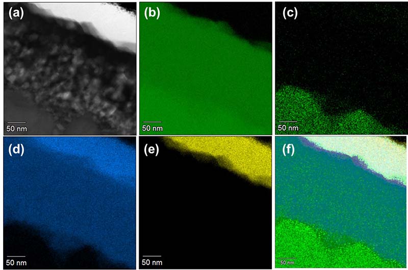
Figure 7:Elemental maps of a region containing GaN layer and oxide layer of 900℃/20min annealed sample. (a) STEM BF image, (b)Ga map, (c)N map, (d)O map, (e)Si map, (f)mixed map.
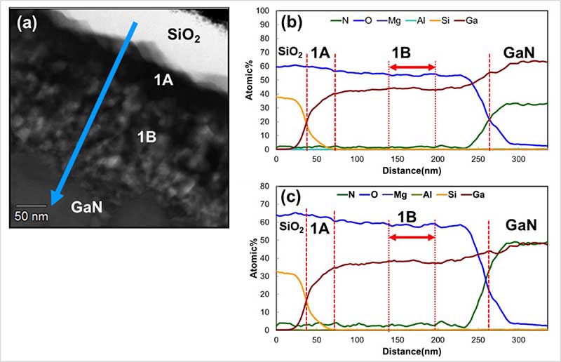
Figure 8:EDS line profiles of a region containing GaN layer and oxide layer of 900℃/20min annealed sample. (a)STEM BF image, (b)EDS line profiles calculated by the built-in EDS program, (c)EDS line profiles calibrated by self-calibration EDS quantitative analysis technique.
In case you have any needs or want to learn more about what it is all about, please contact us at +886-3-579-9909 Ext. 1016│ Email: Js_Bow@istgroup.com;marketing_tw@istgroup.com
References:
[1] H. Hirayama, T. Yatabe, N. Noguchi, N. Kamata, “Development of 230-270 nm AlGaN-Based Deep-UV LEDs,” Electron. Commun. Jpn., 93 (3), 24–33 (2010).
[2] M. Martens, F. Mehnke, C. Kuhn, C. Reich, V. Kueller, A. Knauer, C. Netzel, C. Hartmann, J. Wollweber, J. Rass, T. Wernicke, M. Bickermann, M. Weyers, M. Kneissl, “Performance Characteristics of UV-C AlGaN-Based Lasers Grown on Sapphire and Bulk AlN Substrates,” IEEE Photonics Technol. Lett., 26 (4), 342–345 (2014).
[3] F. Mehnke, M. Guttmann, J. Enslin, Kuhn, C. C. Reich, J. Jordan, S. Kapanke, A. Knauer, M. Lapeyrade, U. Zeimer, H. Krüger, M. Rabe, S. Einfeldt, T. Wernicke, H. Ewald, M. Weyers, M.Kneissl, “Gas Sensing of Nitrogen Oxide Utilizing Spectrally Pure Deep UV LEDs,” IEEE J. Sel. Top. Quantum Electron., 23 (2), 29–36 (2017).
[4] S. M. Islam, V. Protasenko, K. Lee, S. Rouvimov, J. Verma, H. Xing, D. Jena, “DUV Emission at 219 nm from Ultrathin MBE GaN/AlN Quantum Heterostructures,” Appl. Phys. Lett., 111 (9), 091104 (2017).
[5] T. Takano, T. Mino, J. Sakai, N. Noguchi, K. Tsubaki, H. Hirayama, “Deep-Ultraviolet Light-Emitting Diodes with External Quantum Efficiency Higher than 20% at 275 nm Achieved by Improving Light-Extraction Efficiency,” Appl. Phys. Express, 10 (3), 031002 (2017).
[6] T. Y. Wang, W. C. Lai, S. Y. Sie, S. P. Chang, Y. R. Wu, Y. Z. Chiou, C. H. Kuo, J. K. Sheu, “AlGaN-Based Deep Ultraviolet Light Emitting Diodes with Magnesium Delta-Doped AlGaN Last Barrier,” Appl. Phys. Lett., 117 (25), 251101 (2020).
[7] T. U. Wang, W. C. Lai, S. Y. Sie, S. P. Chang, C. H. Kuo, J. K. Sheu J. S. Bow, “AlGaN-based Deep Ultraviolet Light-emitting Diodes with Thermally Oxidized AlxGa2-xO3 Sidewall,” J. ACS Omega, (ACS ID: ao-2022-00813q.R2) (2022).
[8] J. S. Bow, Jay Wang, W. C. Lai , T. Y. Wang, S. Y. Sie, S. P. Chang, C. H. Kuo, J. K. Sheu, “Characterization of Oxide Layers on AlGaN Based DUV LEDs by TEM/STEM Analysis” IPFA 2022 (2022).
[9] G. Cliff and G. W. Lorimer, “The quantitative analysis of thin specimens”, J. Microscopy 103, 203-207 (1975).
[10] J. H. Paterson, J. N. Chapman, W. A. P. Nicholson, and J. M. Titchmarsh, “Characteristic X-ray production cross-sections for standardless elemental analysis in EDX”, J. Microscopy 154, 1-17 (1989).
[11] D. B. Williams and C. B. Carter, in Transmission Electron Microscopy, Chapter 35, (2009)
[12] T. Oshima, T. Okuno, N. Arai et al., “Vertical sola-blind deep-ultraviolet Schottky photodetectors based on - Ga2O3 substrates,” Appl. Phy. Express, 1(1):011202 (2008).
Other services you may be interested in
Ga2o3, Ga2O3,