Issued Date:2022/9/13 XRD materials analysis
Issued By:iST
In an advanced process, while stringent control to verify quality stability is required after materials selection and changes, how to verify the characteristics of new materials?
While the IC size keeps reducing according to Moore’s law to a physical extreme that no further miniaturization is allowed, changing the materials used is the solution. By substituting with materials of more appropriate characteristics, manufacturers can reduce the power consumption and improve the frequency characteristics of components.
As the manufacturing process of semiconductors involves hundreds of procedures, after a materials change, it is also necessary to consider the need for a process equipment change, the usability of samples after the equipment change, and the quality compliance with the original IC design specifications. Hence, when selecting new materials at the development phase and verifying production after materials change confirmation, it is necessary to perform a series of stringent materials analysis and controls to verify compliance with the required characteristics.
In this iST Classroom, we will introduce to you the X-ray diffraction analysis using the X-ray diffractometer (XRD), an essential solution for selecting or changing materials in advanced process development.
XRD materials analysis
XRD materials analysis
XRD materials analysis
XRD materials analysis
XRD materials analysis
X-ray diffraction analysis (XRD) generates a pattern using X-ray and the diffraction of a crystal. By comparing this pattern with the pattern database, we can infer the crystallographic structure, crystallographic array, the size of nanoscale dies, and perform the crystallinity analysis of monocrystal and polycrystal films. It is a non-destructive analysis of materials characteristics.
1. How to improve RD delay to increase IC operation speed?
On principle, the manufacturing process of semiconductor components falls into the front-end, middle-end, and back-end sections, and the interconnect is related to the component operating speed.
To further reduce the resistance-capacitance delay (RC delay) time, lower resistivity interconnect materials and low-κ dielectric insulation materials are the options. In the earlier change to components with nodes at 0.1um, aluminum (Al) was replaced by copper (Cu) to reduce resistivity by about 40%, and process equipment was also changed from physical vapor deposition (PVD) into chemical vapor deposition (CVD). Additionally, different low-κ materials were also used to make improvements.
When the process advanced to nodes below 10nm (N10), further improvement in the electro-migration and heat stability of copper interconnect was impossible in smaller circuits. Figure 1 shows when the pitch of interconnects reduced from 20nm (N5) to 12nm (N3), the circuit was reduced to 2nm when copper in the middle was compressed by the barrier and liner to increase resistivity by nearly 100 times (please refer to Figure 1). Hence, another materials change was required to effectively reduce resistivity.
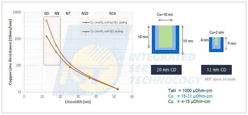
Figure 1:Resistivity changes when interconnect pitches reduces from 20nm to 12nm.
(from Paul Besser, ECS 2016)Manufacturers have been studying the possibility to replace the current internal interconnect barriers with platinum-group metals (PGMs) used in catalysts, such as Ru, Rh, and Pd as shown in the periodic table of elements (Figure 2), and some transition elements, such as Mo and Co. Co was the first metal used for contact plugs and liners.
Hence, how to judge the compliance of the characteristics of new materials at the R&D phase? As these metals must undergo the high-temperature process before processing into films of dozens of nanometers thick or even ultra-thin films, the most fundamental, non-destructive analysis using XRD can help determine if their original physical properties are maintained after the high-temperature process and the association between their crystallization behavior and electronic transmission in order to provide the related characteristics of materials.
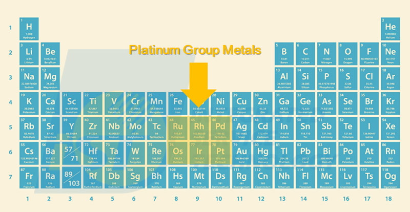
Figure 2: PGMs in the periodic table of elements.
2. How crystallinity of materials affects resistivity
In terms of the crystallinity of materials, besides structural strength, die scale affects electrical property most importantly. In general, the thickness and temperature increase during thick firm formation will affect the die size and reduce the grain boundary. When electrons move faster due to the smaller barrier of grain
boundary, resistivity also reduces.Additionally, although a grain will also grow when the annealing temperature is high, as the interconnect scale is getting smaller, grain growth will be limited, and the direction of crystals will affect the speed of electron flows. Hence, it is exceptionally important to analyze the crystallinity of thin films of a few nanometers thick with grazing incident diffraction (GID).
Recent studies found that Ru and Cu are the most potential options. Ru is characterized by a high melting point and low resistivity, while Cu has good adherence. Therefore, they have become the objects of constant research.
Figure 3 shows the GID patterns of the resistivity at different annealing temperatures and crystallinity analysis of a 40nm-thick Ru thin film. It is clear that Ru (101) is the preferred orientation because the higher the temperature is, the full width of half maximum ( fwhm ) of (101)’s peak is narrower, i.e. as the grain size increases, the corresponding resistivity reduces to support the previously proposed theory.
Figure 4 shows the GID overlay of the ultra-thin Ru film at 5nm grown with atomic layer deposition (ALD) at room temperature and 400℃. It also shows that the Ru peak becomes apparently narrower after high-temperature treatment, i.e. the grain is bigger than the one grown at room temperature.
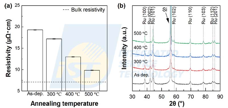
Figure 3: Resistivity (a) and XRD (b) analysis results of Ru thin films at different annealing temperatures.
(from American Chemical Society. 2021, 33, 5639−5651)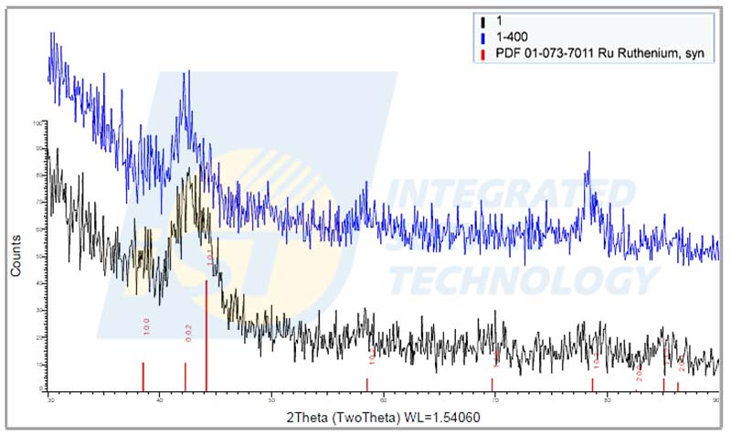
Figure 4:Comparison of the XRD analysis results of 5nm Ru thin films at room temperature and after annealing 400°C.
(from Integrated Service Technology, Inc)3. Measuring the thickness of ultra-thin films related to coating speed
Additionally, the x-ray reflectometry (XRR) in XRD can also analyze the thickness of ultra-thin films grown with ALD. Figure 5 shows the reflectometry of Ru ultra-thin films grown on SiO2 substrates. After software fitting, besides showing that the thickness of Ru ultra-thin film is 4.33nm, the results can also be used to analyze thedensity and the roughness of surface and interface.
Figure 6 shows the number of ALD cycles. The thickness trend measured with XRR shows that the deposition rate is properlyin a linear positive proportion. These results of ultra-thin film analysis using XRR enable quick analysis and study to provide a reference for ALD process improvement.
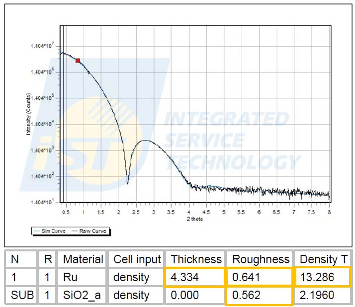
Figure 5:XRR graph and fitting analysis results of Ru ultra-thin films grown with ALD.
(from Integrated Service Technology, Inc)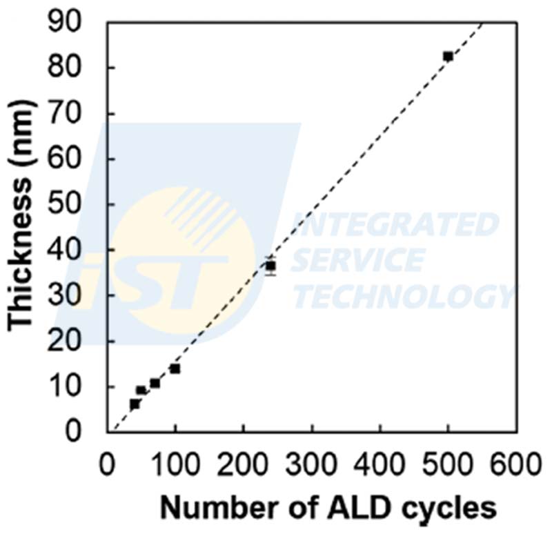
Figure 6:The correlations between ALD cycles and XRR thickness analysis of Ru thin films grown in SiO2 substrates.
(from American Chemical Society. 2021, 33, 5639−5651)4. Non-destructive measurement of plasma damage formed on the surface of Low-k materials
Many process technology R&D may have been conducted on new low-k materials. Low-k materials must undergo dual-damascene etching, PVD metal coating, or surface finish and cleaning. In these processes, chips will be impacted by plasma, leading to serious surface modification. That is, the IC defects extended from plasma damage will cause failure.
Figure 7 shows the O2 (left) and He (right) plasma impacts on low-k materials. The TEM image in Figure 7 (left) shows a darker layer is formed at the upper layer of the low-k SiCOH. Figure 7 (right) shows a high-density compact layer of about 17nm thick formed on the surface, as shown through XRR analysis.
Apparently, XRR fitting can also clearly show the thickness, density, and even surface and interface roughness of this layer after plasma damage. If the sample is used for other experiments afterwards, it cannot be damaged, and XRR is the only analysis tool to meet the needs at the R&D stage.
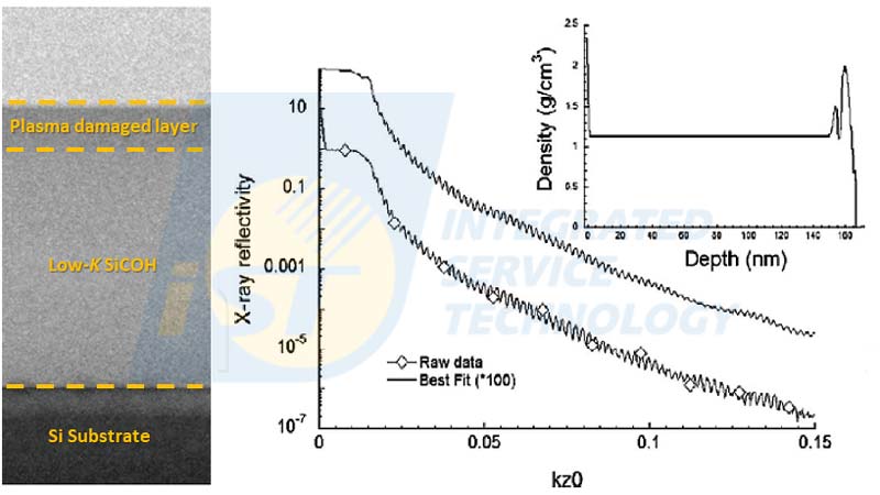
Figure 7: TEM (left) and XRR (right) analysis results of low-k materials after O2 and He plasma damage
http://dx.doi.org/10.5772/intechopen.79494: Plasma Damage on Low-k Dielectric Materials)5. Analysis of residual stress affecting thin film reliability
After repeated deposition of metal coatings and processing with different conditions, it is necessary to verify if there is a stress change in low-k materials. Internal stress is generated due to the density difference of deposition. After the grinding of the subsequent CMP process, when there is stronger stress on a particular location, stripping or cracking will very likely happen. Hence, it is necessary to find out the existing residual stress.
After different depositions, the space between lattices on the thin film will be squeezed or stretched. Hence, the substitute analysis using XRD peak angular displacement measurement (Δ2θ) with the common mathematical model (sin2ψ method) can obtain the residual stress.
Figure 8 shows the residual stress of Ru thin films grown with two different processes obtained with XRD analysis of Δ2θ. Figure 8 (upper) shows the results of Sample A: tensile at 2.06GPa, and Figure 8 (lower) shows the results of Sample B, a smaller tensile at 0.83GPa.
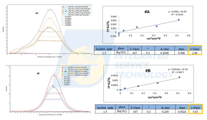
Figure 8:Comparison of the XRD results of residual stress on Ru thin films grown with two different processes.
(from Integrated Service Technology, Inc)
In conclusion, besides benefiting the R&D of the IC back-end process, XRD and XRR can be used to analyze the crystallization quality of rocking curve or RSM in the frond-end epitaxy process using the HRXDR technique. Additionally, XRD-related analysis techniques can help analyze the phase of crystallization of contact silicide, the crystallinity and preferred orientation of compound thin films, the residual stress of polycrystal thin films, and even the thickness, roughness, and density of multi-layer thin films.
In case you have any needs or want to learn more about what it is all about, please contact us at +886-3-579-9909 Ext. 6613 Chiru Chang│ Email: sa_tw@istgroup.com;marketing_tw@istgroup.com
Other services you may be interested in
XRD materials analysis