Issued Date:2022/8/30 IC Cross section
Issued By:iST
There are several methods to section a chip to solve structural issues.
According to the attributes of your samples, which methodology is the best choice?

After IC design, before performing the subsequent functional test, reliability test or failure analysis & debug, it is necessary to run sample preparation by cross-sectioning. This step plays a critical role in verifying all potential defects, including metal interconnection, structures between each layer, solder joint and wire bonding.
There are several ways to observe the cross section, like the conventional grinding (mechanically polish to the layer of observation) or ion beam cross-section polishing. So, what are the advantages of each method? Which method of sectioning is the best for observing your sample? In iST Classroom this time, we will introduce four commonly used methodologies, from nm-sized target (like defects in advanced node) or large area structural observation (like TSV), to help you find the most suitable way for efficient cross-sectioning.
IC Cross section
1. Grinding: Large sample preparation, applicable to an observation area within 15 cm
The biggest advantage of grinding is the applicability to a large area observation (<15 cm), spanning across the entire die, or even the package. So, this method is ideal when running inspection on the entire stacking structure or dimensional measurement (figure 1). Grinding allows an observation on the desired location through four steps: mechanical cutting, cold mount, grinding and polishing (click here to read more).
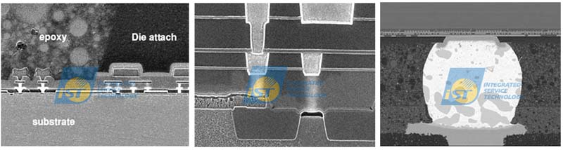
Figure 1 Left image: Die cross-section; figure 1 middle & right images: Cu process cross-section
However, there are two disadvantages of grinding; besides the structural damages like deformation and scratch caused by mechanical stress, the result of this method significantly relies on the execution experiences of the operator (figure 2). An inexperienced operator may damage the target area when over-grinding and thus leads to an undesirable result.
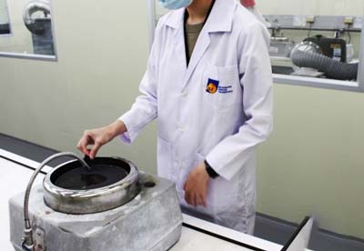
Figure 2: Conventional grinding significantly relies on the execution experience of the operator
2. Cross-section Polisher (CP): Besides cross-section analysis, also applicable to areas requiring gentle-etching
Compared to grinding, the advantage of the cross-section polisher is that this method utilizes ion milling as the ending cut to minimize man-made mistakes as well as the structural damages caused by the mechanical stress of conventional grinding. In addition to sectioning, CP ( IC cross section ) can perform “gentle etching” on specimen surface to solve metal deformation after grinding. If the purpose is to observe the structure of stacked metal or intermetallic compound, CP will be the best choice.
In CP ( IC Cross section ), the sample is grinded close to the target and then Ar+ ion is used to mill to the target area. This method not only reduces analysis time but also offers a complete and clear material contrast under SEM inspection (figure 3).
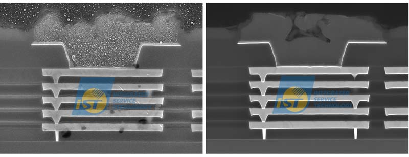
Figure 3: SEM images. Left image: IC structure after grinding; material contrast between each layer is unclear. Right image: IC structure after cross-section polishing shows clear boundary between each layer.
● Case 1: Cross-section polishing for fast and efficient analysis
The sample for test is in BGA package; it only takes one hour to section when it is necessary to analyze a specific bump through CP over1 mm range. Using SEM, the material distribution on solder balls can be clearly revealed (figure 4).
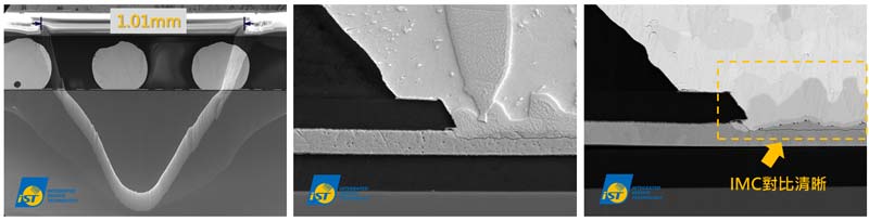
Figure 4: SEM images. Figure 4 (a): the cross section after CP; the entire bump is clearly revealed. Figure 4 (b): BGA after grinding; though the IMC of the bump can be viewed, but it is difficult to show clear boundary of IMC due to metal deformation after grinding. Figure 4 (c): BGA after cross section polishing; the comparison of IMC is clearly revealed for material contrast.
● Case 2: Improved copper deformation through CP milling
In a common PCB stacked via structure, a weak bonding between the blind via hole (BVH) and Cu layer can lead to in-between cracks after the thermal treatment process and thus cause unstable resistance. A general solution to this is to examine by grinding; however, such solution tends to cause copper deformation and affects the judgement. Instead, CP is a more suitable choice here; running CP milling on BVH structure can efficiently solve this issue, and this method is applicable to a width over 10 mm (figure 5).
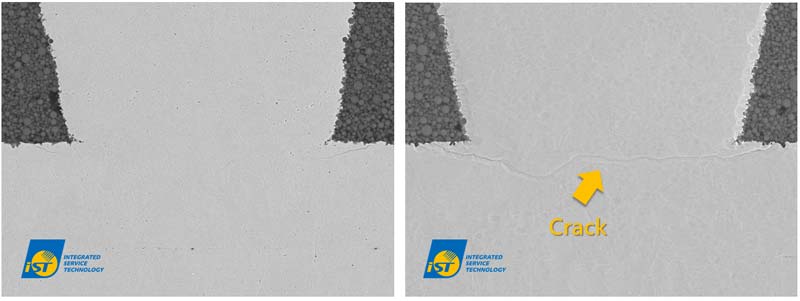
Figure 5 Left image: PCB via after grinding; the crack is invisible. Figure 5 Right image: PCB via after CP milling; the crack is clearly revealed.
3. Plasma FIB (PFIB): The choice for local analysis without damaging the entire sample
In 3D IC package sample, if you does not want to damage the entire sample by grinding, you can consider “PFIB”, a tool integrating plasma milling and SEM observation and applicable to a range of 50–500 um. This tool is suitable for cross section analysis as well as delayering observation (Further reading: Improved delayering techniques for better fault isolation efficiency of advanced process chip); one can even mill while observing a specific area, without worrying about damaging the target area by mistake. The integrity of a defect or specific structure for observation can also be maintained (figure 6).
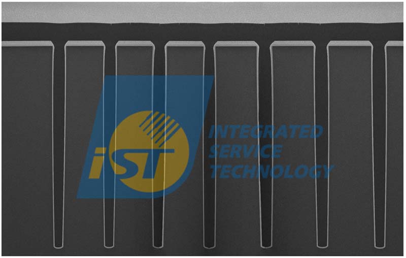
Figure 6 shows the TSV structure after PFIB milling. Except accurate measurement of metal coating thickness, it also enables a clear measurement of CD (critical dimension) of TSV after etching as there is no mechanical stress compared with grinding.
4. Dual Beam FIB (DB-FIB): Applicable to local cross section analysis of a few-nm-sized area
DB-FIB, integrating Ga-ion beam and SEM, can perform a nm-scale localization and observation on micro structure in the sample (figure 7) and is applicable to an analysis or defect observation on a structure under 50um. This method also allows the information related to composition and crystalline in the target area to be acquired by EDX and EBSD (electron backscatter diffraction) analysis, respectively. In addition to the aforementioned analyses, when it is not possible to acquire sufficient information by SEM as the size of the target reaches the resolution limit, DB-FIB can also be applied to TEM sample preparation to facilitate an analysis with a higher resolution.
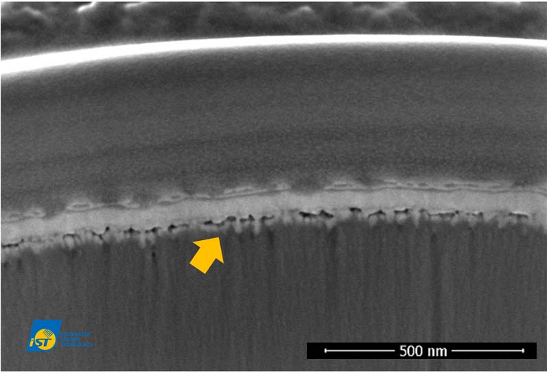
Figure 7: Combine SEM and a gallium ion gun, DB-FIB can perform defect localization and microstructure analysis.
We hope the introduction in iST Classroom this time helps you with a more thorough understanding of cross-sectioning methods as well as more applications, including more CP milling applications. PFIB with delayering capability also opens up another door for failure analysis methodology against advanced node. We are glad to share the expertise and our experience with customers supporting iST all the time. For related knowledge or more advantages about each analytical equipment, please don’t hesitate to email iST and we will prepare a detail compared table regarding four commonly used analytical equipment for reference. For more information, please call: +886-3-579-9909 #6775, Mr. Shih, or send your email to: web_ise@istgroup.com , marketing_tw@istgroup.com
Other services you may be interested in
IC Cross section