Issued Date:2021/11/2FCQFN
Issued By:iST
How to quickly pinpoint defects of a FCQFN, a kind of power ICs, with failure analysis tools?
Being without leads from four sides, the Quad Flat No leads (QFN) packaging ends up with products featuring compactness, low costs and good heat dissipation. This is driving the packaging industry trending toward QFN to adapt to high computing and miniaturization aimed by the IC design houses. The QFN technology is getting adopted by high speed communication ICs, power management and Wi-Fi chips for wearable, handheld devices and electric vehicles.
A Flip Chip QFN (FCQFN) is a QFN packaged with flipped chip. It features a shorter electrical path (relative to QFN), smaller high-frequency attenuation, rapid signal rise and better electrical performances. All these are making it the more advanced packaging type now.
FCQFN
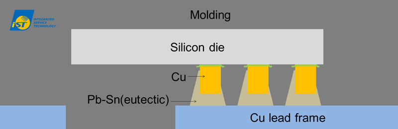
Figure 1: Structure of FCQFN
The lead-free features come at costs of more doubts on soldering quality as it’s getting harder to judge from the appearance of solder joints. Moreover, risks of poor reliability like solder cracks and other issues may get higher since FCQFN not only uses copper pillar and tin connection to replace the wiring bonding of traditional QFN, but its structure is more complex than QFN.
Addressing this, this iST Classroom is sharing with you how to pinpoint the defect position quickly with the iST’s five steps.
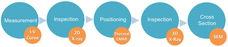
Figure 2: The iST’s five steps for locating the defects of FCQFN
Step 1: I-V Curve
Identify IC’s electrical characteristics anomalies (including Open, Short, Leak and High Resistance) by I-V Curve.
Step 2: 2D X-Ray Inspection
When the electrical characteristics anomalies is confirmed, inspect packaging structure defects with the 2D X-Ray ; this package structure image will be also used to confirm the defect location in the subsequent analysis.
Step 3: Position Hot Spot by Thermal EMMI
Position hot spots with thermal EMMI (InSb) by receiving the phase differences of thermal radiation generated from a defective point without hampering the original situation of the sample. Then, overlay these positions on the package structure image by 2D X-Ray in step 2 to locate the defects, see Figure 3 for details.
Please note that the thermal EMMI can reveal the depth of defects (in Phase value shown by equipment readings) by IC packaging. The Phase value of hot spots on the normal die ends in this case is 77.1 while that of the abnormal bright one is 78.5. Since these two are very close to each other it’s safe to assume that the defects may lie on the die end of the copper pillar rather than the lead one.
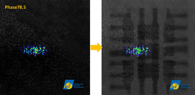
Figure 3: Use thermal EMMI to position hot spots (see figure on the left) and overlay the 2D X-ray one (see figure on the right) to locate the could-be defect.
Step 4: 3D X-Ray CT Analysis
To verify the assumption, the iST lab performs CT (Computed Tomography) analysis by cutting the internal structure layer by layer over the defects with 3D X-ray (Figure 4) to identify where defects are located.
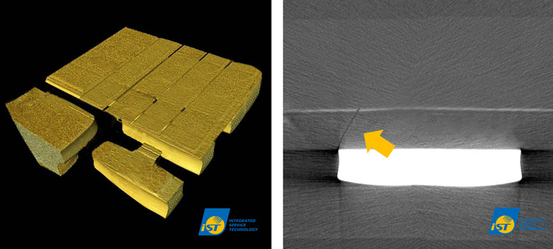
Figure 4: Identify which layer the defects are located by CT analysis with 3D X-ray
Step 5: Pinpoint the Location of Defects by X-S and SEM Cross Section
The next is to pinpoint the location of the defects once the layer they lay on has been determined in step 4. The iST lab grinds into the defect points from the side in step 5. Inspect by SEM found failure of the crack on the die end of the copper pillar as shown in Figure 5.
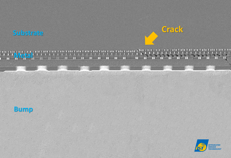
Figure 5: Inspect by SEM to locate cracks on the die end of the copper pillar
In case you have any problems with the IC failure analysis or want to learn more about what it is all about, please call Mr. Shih(CY) at +886-3-579-9909 Ext. 6775 or send him an email at web_ise@istgroup.com.
Other services you may be interested in
FCQFN