Issued Date:2021/7/27Low Temperature Soldering
Issued By:iST
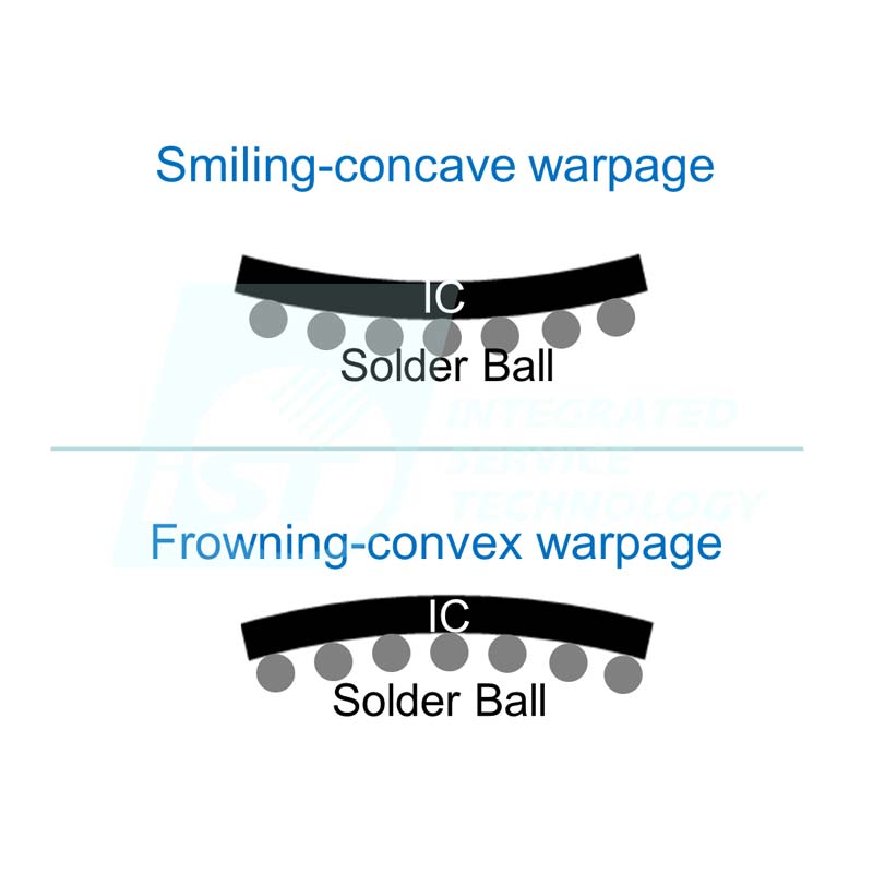
Reliability test failed after ICs mounting on PCB due to non-wetting and early failure caused by warpage.
Are there any special processes able to reduce warpage deformation?Low Temperature Soldering
What frightens IC designers the worst is that ICs of good quality failed the verification once surface mounted on PCBs. This has been the case with many clients of the iST lab for board level reliability (BLR). iST found most of these issues are contributed by warpage after surface mounting these days. Further to early failure in reliability tests, in the worst cases you may have to return the product back to its initial IC design phase of development and waste many days before launching the product.Low Temperature Soldering
Why is the frequency of warpage-relevant reliability issues soaring now? The trending “system in a package” can be blamed, according to the iST’s BLR lab. Integrating ICs of different materials, usually containing substances with varying coefficient of thermal expansion (CTE), and functions into one package is set to lead to warpage by stacking complex and diversified packaging components. This has been the greatest challenge faced by raising the yield of the surface mount technology (SMT).
Low Temperature Soldering
Low Temperature Soldering
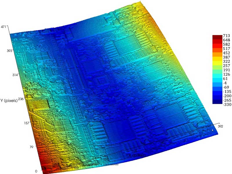
Figure 1: Chips by advanced process come with warpage more or less. Quality of them after surface mounted on PCBs remains OK as long as the level of deformation compliant with the IPS specifications (source: Akrometrix)
Conventional Method – Slightly Relieve Joints From Stretching or Squeezing by Adjusting Solder Pastes Applied with Data Simulation
Regarding warpage-relevant non-wetting, the iST BLR lab is cutting the probability of warpage-relevant non-wetting and short circuit by adjusting the design of solder paste’s stencil and reflow temperature based on results of warpage simulation (Figure 2). iST has been working with many clients to deal with the soldering issues of PCBs or IC warpage. (Read more: Count Warpage Amount Before SMT to Avoid Solder Empty and Early Failure)
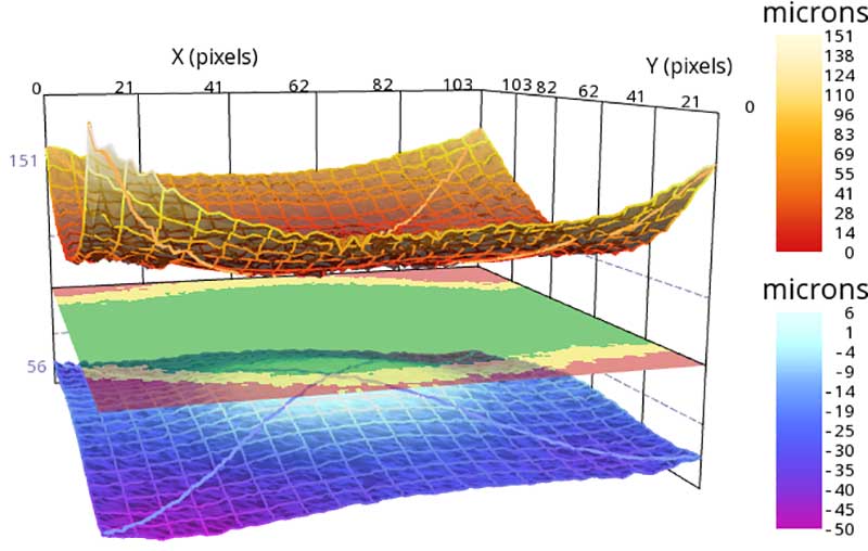
Figure 2: Learn about warpage by simulating and analyzing components and PCBs before surface mounting (source: Akrometrix)
New Method – Reduce Level of Warpage with Low Temperature Soldering (LTS) Process
The aforementioned method, preventing non-wetting or short circuit by applying correct amount of solder pastes, doesn’t work when the level of warpage gets higher.
Regarding this issue, here comes the new method of low temperature soldering (LTS) by the iST’s BLR lab to reduce level of warpage deformation with less thermal stress.
■ What is LTS
The melting temperature of tin, silver, and copper alloys used by most Pb-free processes is about 220℃ (with peak values falling in the range 230℃~250℃) while that of tin and bismuth alloys used by LTS process is 140℃ (with peak values falling in the range 170℃~200℃), see Table 1 and Figure 3.
Table 1: Melting point and peak temperature of most Pb-free and LT soldering
Pb-free process LTS process Melting temperature 220℃ 140℃ Peak temperature 230℃~250℃ 170℃~200℃
(vary with ingredients of solder paste)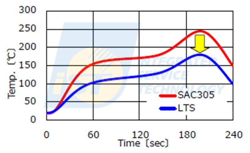
Figure 3: Reflow profile with the blue line for the LTS process and red for the Pb-free one
■ Why Can the LTS Process Reduce Level of Warpage Deformation?
Warpage is the results of deformation by soldering substances of different CTEs when stacking ICs made of different materials. The higher the temperature is the IC package will suffer more deformation by thermal stress (Figure 4). Lower SMT soldering temperature would reduce thermal stress significantly which, in turn, would not only reduce warpage suffered by PCBs and components but also cut energy consumption.
Figure 4: The higher the temperature the greater the deformation
Use the LTS Process to Get Around the Challenge Faced by SMT
■ Prevent hot tearing due to soldering heterogeneous alloys by controlling temperature and solder paste volume
Pb-free process is used for component packaging in most cases now. That is, bumps and solder balls remain made by tin, silver, and copper alloys, e.g. solder bars SAC305, SACQ, and SAC405. Solder joints by LTS process differ greatly as its temperature went below that of the tin, silver, and copper alloys (see Figure 5 and 6).
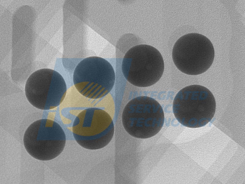
Figure 5: SAC solder balls collapsed after solder balls and pastes fully melted by reflow of Pb-free process
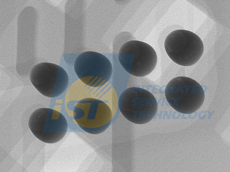
Figure 6: Partially melted SAC solder balls didn’t collapse after LTS process reflow
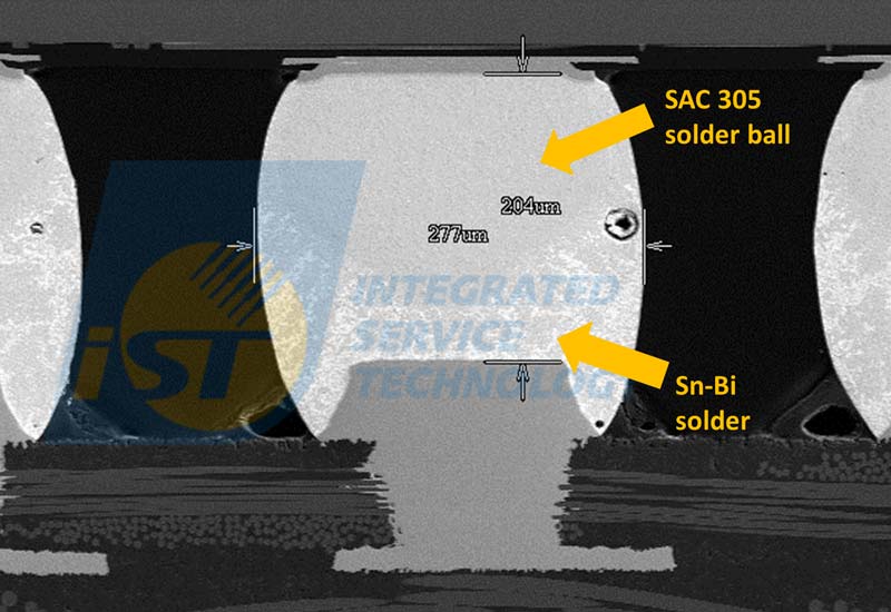
Figure 7: Cross section of solder joints with precision controlled soldering temperature and solder paste volume
By precision control of temperature and solder paste volume, the iST’s BLR lab is able to prevent hot tearing encountered by the LTS process. Take Figure 7 for example, joints by solder paste of Sn-Bi alloys and SAC305 solder balls come with good diffusivity yet without hot tearing under appropriate solder paste volume and controlled reflow temperature.
■ Practices in Improving Product Reliability with LTS Process
Joints between different alloys may lead to early reliability test failure due to poor molecular diffusion. Thus, the iST BLR lab subjects samples of small-size WLCSP with heterogeneous alloys soldering by LTS process for subsequent reliability verification. The result of temperature cycle test (TCT) suggests that samples by LTS process rival their Pb-free counterparts in terms of TCT reliability test.
It’s clear that the combination of SAC305 bumps with LTS solder pastes (either Sn-Bi-Sb-Ni or Sn-Bi-Ag) may rival that of SAC305 bumps and SAC305 solder paste in terms of TCT test as shown in Figure 8.
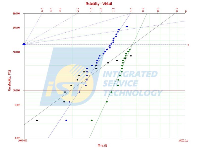
Figure 8: Compare the results of TCT tests over SAC305 solder ball samples by Pb-free and LTS process. In general, SAC305 solder paste is used in the Pb-free process (blue line), while solder paste of Sn-Bi-Ag (black line) or Sn-Bi-Sb-Ni (green line) is used in LTS process.
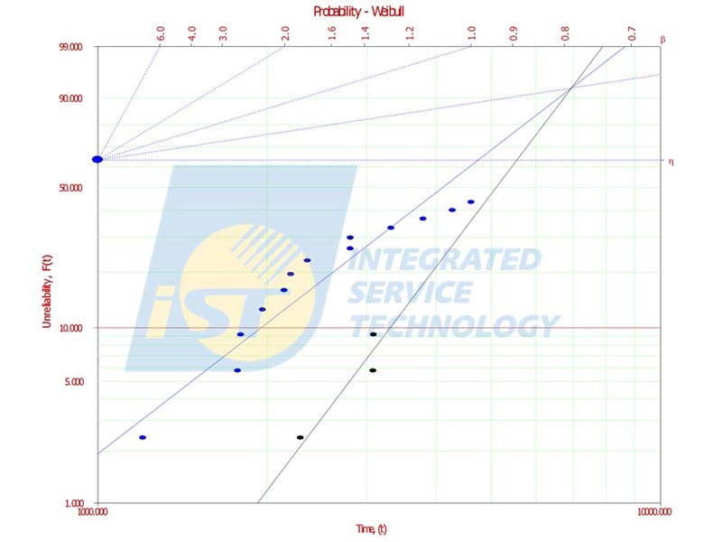
Figure 9: The results of TCT tests over different proportion of solder paste in LTS process. The blue line represents the use of less solder paste, and the black line represents use of more solder paste.
LTS process remains an acceptable method to reduce warpage as long as the CTE issues cannot be solved by packaging materials. The actual application may include other active and passive components such as chip resistors, capacitors, memories, and transistors. All of them should be ready at the earliest for quick products launch. This is to share experiences of iST with you. To learn more about the LTS process, feel free to call Sam at +886-3-579-9909 Ext. 6433 or email him at WEB_SMT@istgroup.com and marketing_tw@istgroup.com.
Other services you may be interested in
Low Temperature Soldering