Issued Date:2021/1/21Underfill Void
Issued By:iST
Underfill Void
Do the voids caused by poor underfill process hinder you from having accurate reliability performance and lifetime estimation for advanced IC package?

The reliability of solder joints with ball pitch smaller than 0.25mm is getting more attention as fine pitch packaging technology has increasingly been applied on packages such as BGA (Ball Grid Array) and CSP (Chip Scale Package).
However, the stress from thermal and mechanical (e.g. bending or shock) tests could cause cracks in fine pitch solder joints, which may lead to failure.
To improve the reliability of chips, adding an underfill process after SMT (Surface
Mount Technology) can effectively prevent solder joints (the weakest part in the entire structure) from failing due to stress.
In the underfill process, epoxy is dispensed at the edge of a chip and then fills up the gap between solder joints by capillary action.
After the underfill is cured, it can improve the mechanical strength of solder joints and extend the service life of chips (Figure 1).
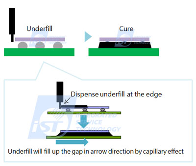
The underfill process is frequently adopted by hand-held devices, e.g., PCBs in smartphone or tablet, as they have to go through demanding mechanical shock and vibration tests. Otherwise, the solder joints of chips are very likely to fail these two tests.
Voids, more or less, may occur in the said process due to factors including bubbles in the underfill tube, dispensing temperature and pattern, temperature curing parameters, solder ball matrix, ingredients of solder paste and flux, etc. The above-mentioned items may hinder the underfill from wrapping around the solder balls at chip bottom and lower the effectiveness of protecting solder joints.
In this iST tech classroom, we will share two cases about where voids are most likely to appear in the underfill process and how they affect the reliability of chips.
Case 1: Underfill Flow Obstructed by Flux Residue from SMT Process
iST reliability verification lab found that flux residue may block the path of underfill flow (see Figure 2) and obstruct the epoxy from filling up the chip bottom. The underfill process in this case could result in many voids.
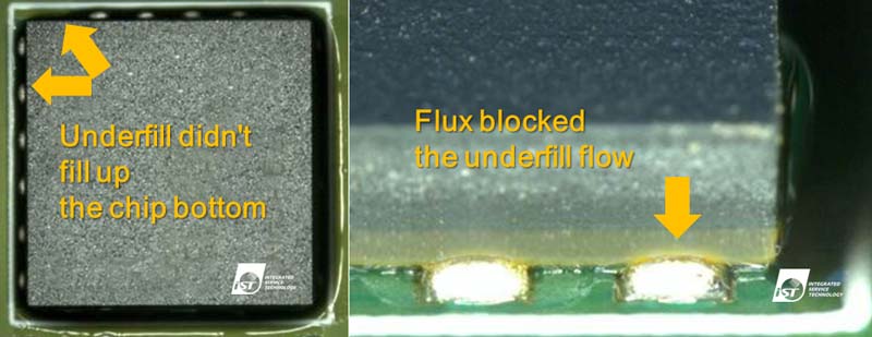
Figure 2: Flux blocks the flow of underfill
Therefore, we suggest performing flux cleaning to remove foreign matters and then bake the PCBA before moving on to the underfill process (see Figure3).
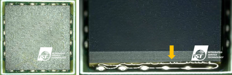
Figure3: Underfill fills up chip bottom after flux cleaning
Case 2: Underfill Fails to Wrap Around Each Solder Joint
As the chips are getting smaller due to advanced package process, the pitch between solder balls has also been reduced. The distance between the substrate and the die has shrunk to 10-30um. The smaller the pitch is, the slower the flow rate will be.Underfill Void
This makes underfill harder to flow and wrap around each solder joint evenly, which, eventually, leads to voids (see Figure 4).
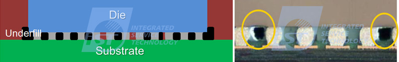
Figure 4: Underfill fails to wrap around each solder joint and results in voids.
What will happen if voids form at the chip bottom? iST reliability lab performed tests and found that samples subjected to high temperature, humidity and bias environment could induce the growth of dendrites along the underfill voids (see Figure 5), which may result in solder ball bridging and abnormal resistance in the reliability tests. Therefore, a longer chip lifetime can be expected if without voids in the underfill.
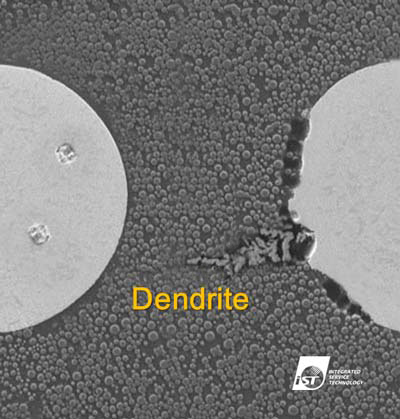
Figure5: dendrite
How to Deal with Annoying Underfill Voids?
Underfill Void
iST reliability lab introduces a vacuum pressure oven, which can adjust the vacuum and pressure parameters according to the viscosity of different underfills to achieve the best quality of zero void in the underfill process and prevent the void from affecting the reliability test results (see Figure 6).
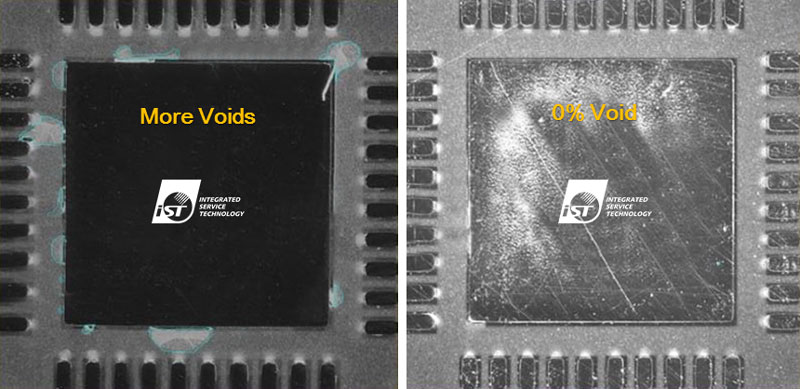
Figure 6: Voids remain in chip by using general oven (left) vs. zero void in chip by using pressure oven (right)
This article is intended to share our experiences with valued clients like you. Should there be any inquiry for underfill process on a small batch of parts or if you would like to know more about the aforementioned techniques, just ring Mr. Chang at +886-3-579-9909 Ext. 6429 or email him at WEB_SMT@istgroup.com.