Issued Date:2020/03/10Tim-Defect
Issued By:iST
Advanced packaging and heterogeneous integration are hot topics now, the quality of TIM is even more so.
How to find out defects of TIM quickly?
Tim-Defect
“TIM (Thermal Interface Materials)” has been the key to the long useful life of high-power advanced packaging products which, in turn, is determined by its coverage rate and actual adhesion.
You must have been concerned by product failures, e.g. delamination and voids, due to poor TIM.
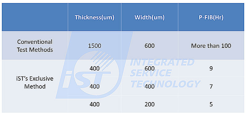
It takes 100 hours or more to inspect defects in samples by Plasma FIB as the lid usually comes at some 2000um thickness in soft TIMs.
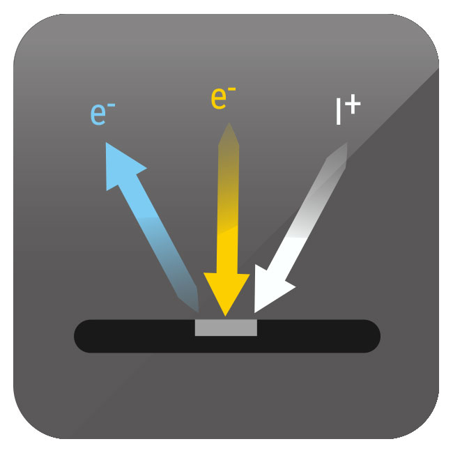
With Xe+ ion source, this Plasma FIB outruns its Ga+ sourced counterpart (Dual-Beam FIB) with up to 20 times the etching speed. Along with high-resolution SEM, it enables watching-when-cutting to pinpoint Nano-scale features or defects in a range of hundreds of microns.
The iST’s exclusive methods prepare samples in a unique way to thin the lid before cutting defects with Plasma FIB. This reduces the analysis time to less than 10 hours and is 10 times faster (see table 1).
Table 1: iST’s exclusive methods V.S. conventional test methods
Three Steps to Identify TIM Defects
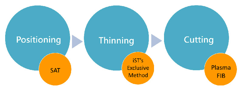
Figure 1: The iST’s exclusive test methods for TIM defects finding
The iST’s exclusive test methods: position the defect with SAT, thin the lid with the iST’s exclusive sample preparation method to about 300~400 um thickness, cutting defects with Plasma FIB to get a clear picture of the TIM .
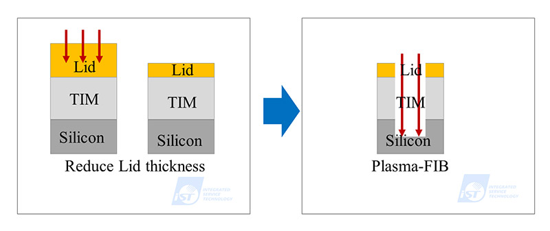
Figure: iST’s exclusive operation methods
Should you have any inquiries for testing methods or any further requirements, just ring Mr. Chen at +886-3-579-9909 EXT 6767 or email us at web_ise@istgroup.com.