Issued Date: 2019/1/8
Issued By: iST
The FSM process includes Electro-less Plating and Sputtering Deposition, which process is more mature, stable, and extremely reliable? Which process has higher capability, price value and shorter production time?
The iST Tech Classroom last month told us that the Sputtering Deposition Process is mature and stable and requires multiple processes including high vacuum sputtering, photo lithography, and etching, which has long been adopted by many car electronics and high-end application manufacturers.
On the other hand, for the cost-oriented consumer products, Electro-less Plating is a good choice with its lower cost and shorter production time.
In addition, the Electro-less Plating process has one critical feature: it can grow NiAu or NiPdAu selectively on Al pads with a series of redox reactions instead of high vacuum sputtering / lithography / etching at lower costs and shorter production times, making it the best choice for high C/P value of MOSFET FSM. In the iST Tech Classroom this month we are going to detail the Electro-less Plating process for you.
I. The Critical Starting Point of Electro-less Plating Pretreatment
(1) Cleaning and Etching of Al pads
The key steps in pretreatment are cleaning and etching of Al pads. This step will remove organic residue and native oxides on pad surface. At the same time, to wet it into a hydrophilic state while etching the Al pads slightly to ensure its reaction with the zinc activator later.
It’s critical to fine tune pretreatment for different Al pads provided by different foundries. If pretreatment is not fine-tune, Al pads may suffer severe losses and pores as shown in Figure 1. These pores may trap nickel in them and lead to interface connection failure in reliability tests later. In case of good pretreatment the Al pad may get etched dense and uniform as shown in Figure 2.
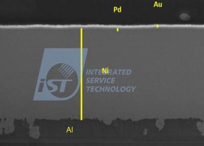
Figure 1: Poor pretreatment may lead to heavy Al pad loss
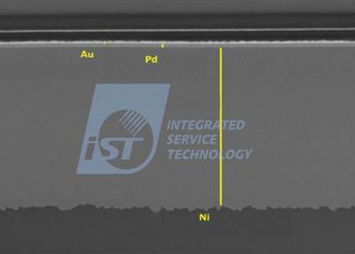
Figure 2: Good pretreatment gives Al pad dense and uniform etching
(2) What to do with under-etching for a pad opening by a front-end foundry?
Pad opening by a front-end foundry is another key step. Cases of iST customers tell that poor pad opening with under-etching may result in the thickness of nickel growth falling below specification. By improving the pretreatment process, iST helped them to go successful Electro-less Plating while their rivals failed to do accordingly. All these signify the importance of pretreatment.
Pretreatment is virtually determining the Electro-less Plating process from the very beginning. Poor pretreatment may result in abnormal zincation and NiPdAu deposition. The experienced front-end process integration team of iST can fine tune the pretreatment process addressing individual products and provide customers with reliable Electro-less Plating process.
II. Zincation
(1) First Zincation
After pretreatment, the robot arm of the machine auto delivers cassettes to the 1st zincation tank for reaction as illustrated in Formula 1 below. Aluminum is oxidized into aluminum ions Al3+ and dissolves in solution while zinc ion Zn2+ is reduced into zinc which film on the Al pad surface.
2Al + 3Zn2+ ⇋ 2Al3+ + 3Zn (Formula 1) (2) Second Zincation
The 2nd zincation process follows after coarse zinc activated particles on rough surfaces are removed by nitric acid. The Al pads are then subjected to the second zincation process to get more compact and condensed surfaces. This 2-step zincation process is now adopted by most Electro-less plating contractors as standard for better surface morphology note 1.
III. Deposit NiAu or NiPdAu
(1) Nickel Tank Employs Online Monitoring System
It’s time to deposit NiAu or NiPdAu once the pretreatment and zincation process has been done. Electrons generated by the reaction of hypophosphite and water in the nickel bath ionize zinc into zinc ions and deposit nickel and phosphorus ions reduce into the nickel and phosphorus on the Al pad as shown in formula 2, 3, and 4. Thanks to the catalytic ability of nickel, the subsequent palladium coating goes on as long as the appropriate chemicals are provided at the end of the nickel plating.
H2PO2– + H2O → H2PO3– + 2H+ + 2e– (Formula 2) Ni2+ + 2e– → Ni (Formula 3) H2PO2– + e– → P + 2OH– (Formula 4) The nickel bath is very critical and needs to be closely monitoring. The iST technical team is very experienced in e-less and related BGBM process. iST builds an In-situ Monitoring System in the bath while setting up the process to enable auto nickel sampling by the system for auto pH value test and absorption rate measurement by a photoelectric colorimeter. The accompanied auto-doping system continuously tunes the chemical solutions in it to facilitate the stable filming process later.
Subsequent palladium and gold tanks employ hypophosphite to generate electrons respectively and deionize palladium and phosphorus ions into palladium and phosphorus, while the complex of gold sulfite in the gold tank grows gold on nickel or palladium with the help of hypophosphite.
(2) Killer of NiAu or NiPdAu Growth: Poor Plating and Over Plating
Lots of manufacturers have been certified successfully and go to mass production stage. Take customer A and B for example, wafers made for both looks uniform in color as shown in figure 3; Al pads observed with a microscope show no sign of poor plating or over plating as shown in figure 4.


Figure 3: Electro-less plated wafer by company A and B
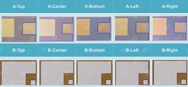
Figure 4: Appearance of Al pad after Electro-less Plating
IV. Takeaways of the Electro-less Plating process
The Electro-less Plating process as summarized in figure 5 is composed of the following steps: pretreatment, 1st zincation, removal of coarse zincated particles with HNO3, 2nd zincation to form fine zincated particles, and finally growth of NiAu or NiPdAu.

Figure 5: Electro-less Plating flow chart
The wafer thinning process starts after the Electro-less Plating process has done. iST is the only one company capable of combining Electro-less Plating and BGBM, CP, and die processes. With this comprehensive one-stop service, wafers finished with front-end foundry processes can be delivered to iST for die processing service.
This article is aimed to share our experiences with honorable clients like you. In case you want to know more details, please call Mr. Yu(Stan) at +886-3-579-9909 Ext. 5888 or email: web_sp@istgroup.com
Note 1: Refer to JH Lee, IG Lee, T. Kang, NS Kim, and SY OH, The Effects of Bath composition on the Morphologies of Electroless Nickel Under Bump metallurgy on Al Input/Output Pad, Journal of Electronic Materials, Vol. 34, No. 1, (2005).