Issued Date: 2018/7/19
Issued By: iST
How to perform FIB circuit edit when the circuit layer of a WLCSP IC is covered by the bump and the RDL (redistribution layer)?
What is WLCSP (Wafer-Level Chip Scale Package)? The aim of WLCSP is to finish IC packaging directly on the wafer using bump as a contact before the wafer is cut. Compared to traditional wire bonding packaging, WLCSP can effectively reduce packaging size. With the rise of wearable and smart handheld devices, WLCSP featuring smaller and thinner packaging size meets the trend of being slim and lightweight, thus fulfilling the demand of increasing clients.
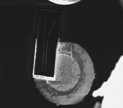
However, IC products packaged with WLCSP are confronted with two big challenges in FIB circuit edit. Most parts of circuits at the lower layers of an IC are covered by the bump and the RDL (redistribution layer) and cannot be edited. Even if there are circuits not covered by the bumps and RDLs, as the organic passivation on top is thicker, greater effort and more time is needed to edit these circuits (see figure 1).
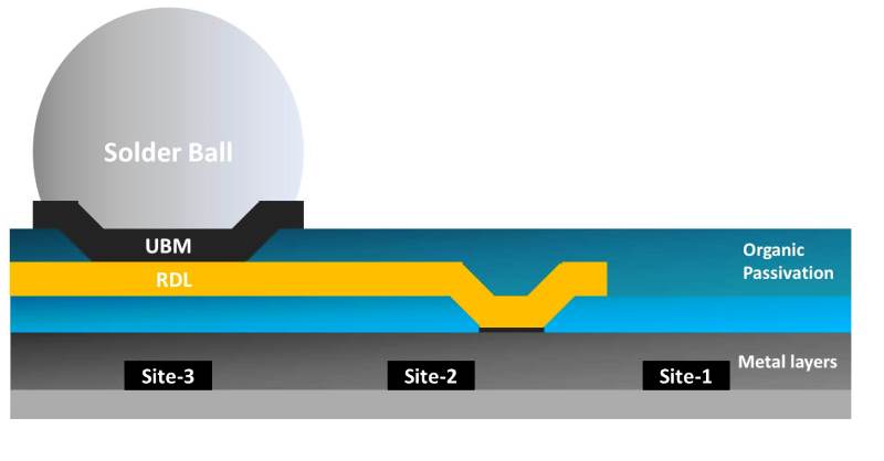
Figure 1: With specific preprocessing engineering methods, FIB circuit edit any sites covered by the bump (site 3), RDL (site 2), or organic passivation (site 1) can be achieved without problems.
To address this issue, iST has developed the solution for WLCSP IC with specific etching technique. FIB circuit edit any sites covered by the bump (site 3), RDL (site 2), or organic passivation (site 1) can be achieved without problems. This technique has been assisted IC design companies around the world, including power management, analog IC, multimedia IC design companies in solving the problem of performing more than 4,600 WLCSP circuit edits in 2,450 cases.
iST Tech Classroom: out of 2,450 circuit edit cases (more than 4,600 WLCSP ICs) we have come up with the following FAQs.
Q1: The location of WLCSP IC circuit needs to be edited is covered with solder balls. After edited by iST, can these balls be used in future?
This may be answered in two dimensions.
Dimension 1: the desired circuit edits are located at the edges of the solder balls.
In cases like this, iST may apply a partial solder ball removal technique which keeps the ball height intact and maintains a certain amount of solder to enable the sample for socket mounting or PCB soldering for electric tests after circuit edit.
Dimension 2: the desired circuit edits are located below the center of the solder balls.
In cases like this, iST may remove the ball and implant a new one after circuit edit for you to go on with follow-up lab tests seamlessly.
That is, the WLCSP solutions by iST are guaranteed to maintain normal solder ball function and testing.
Partial solder ball removal by iST
In case desired changes are located at the edges of solder balls, it is OK to remove part of them to perform the FIB circuit edit, and proceed with circuit testing by immediate PCB soldering or socket mounting to speed up the debugging process.
Whole solder ball removal by iST
In case desired changes are located at the center of solder balls, iST may remove the entire ball to perform the FIB circuit edit, and implant new balls with a Laser Re-ball technique for improving circuit edit feasibility and success rate.
Q2: Can WLCSP IC samples after FIB circuit edit and soldering test be subjected to another circuit edit?
Yes. WLCSP IC samples removed from the test board after a soldering test for another FIB circuit edit may suffer broken solder balls on ICs. The first step is to fully remove the broken solder balls on WLCSP surface before proceeding with the second FIB circuit edit. iST shall implant new balls with a Laser Re-ball technique afterward to enable you to go on with follow-up electric testing.
Q3: How can I replant solder balls without any impact on the accuracy of later reliability verification?
Solder ball replanting was exercised by manual ball placement before heating them to solder to the under barrier metal (UBM) layer of WLCSP IC. This is not only time consuming, but also tends to delamination as a result of the expanding moistures embedded in the PCB due to heated products on the PCB substrate (e.g. BGA package type ICs). This hampers the accuracy of later reliability verification.
Addressing this issue, iST has implanted solder balls with the Laser Re-ball technique to improve operation efficiency and circuit edit success rate.
This article aims to share our experiences with clients like you. Should there be any difficulties in FIB circuit edit inquiries or demand for re-planting solder ball, or you would like to know more about the aforementioned techniques, please call Mr. Wang (Chino) at +886-3-579-9909 Ext. 6092 | web_fib@istgroup.com; or Mr. Chiu (Shaun) at +886-3-579-9909 Ext. 6780 | web_EFA@istgroup.com