Issued Date: 2018/06/29
Issued By: iST
MOSFET component is behind the requirement, however IDMs are at full capacity. What can you do about the long delivery period?
Finally you finish wafer thinning and surface process, but you need to take risk transporting wafer to another suppliers for CP and sawing, is there a place to do it right once?
MOSFET (Metallic Oxide Semiconductor Field Effect Transistor) becomes the inevitable power component of automotive electronics and EV (electric vehicle) to cope with the diversified applications of automotive electronic products and the higher request for low power consumption. In current market, customers have run into a problem of short capacity of MOSFET, however, there happened to be a lack of wafer thinning and surface process services available for customers between the foundry and packaging operations.
Thus, iST has decided to tap into the MOSFET wafer process field, mainly because when iST has gradually become the leading automotive verification laboratory, the company has found this missing part. iST started wondering if they could provide not only services including wafer thinning and surface process services, but WLCSP (wafer-level chip scale package), CP(chip probing) and DPS (Die Processing Service), so that to speed up the delivery of MOSFET components and reduce the risk of wafer transport.
Therefore, iST’s new business– “MOSFET Wafer backend process integrated services” was born, containing special processing services needed between front-end wafer foundry and back-end packaging operations, which are available not only for mainstream 8-inch but 6-inch wafers, including front side metallization (FSM), BGBM wafer thinning, backside grinding (BG) and backside metallization (BM). What is worth mentioning that iST is the only source in current market which is capable to provide both electroless-plating and sputtering services specific to FSM, so as to create the integrated solution for customers.
iST’s wafer backend process integrated services additionally combine downward services including WLCSP, CP and DPS in cooperation with iST’s subsidiary, Innovative Turnkey Solution (ITS), so that an one-stop MOSFET backend solution is ready provided to customers with benefits like speeding up the delivery of MOSFET components and reducing the risk of wafer transport.
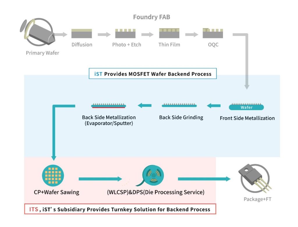
Image: Semiconductor manufacturing process. iST is capable to provide one-stop MOSFET backend solution including WLCSP, CP and DPS in cooperation with its subsidiary, ITS (see the green highlight for iST& ITS services).
If you would like to know more about the aforementioned techniques, feel free to contact Mr. Yu at +886-3-579-9909 Ext. 8802 or email him at Email: web_SP@istgroup.com.