Issued Date: 2017/8/17
Issued By: iST
Computer simulation of device on-board stress-match is normal but the reliability test fails. Is this a device -PCB matching issue or rather that the packaging solder ball lacks durability?
Perform a reliability test on a device with process change; results show an anomaly in high resistance; how to identify the failure point?
In the current month Tech Classroom, iST will share a case of a failure of a Wafer Level Chip Scale Packaging (WLCSP) device that occurred after an on-board reliability test. This is also a frequent failure seen in solder-ball packaged ICs.
The so-called WLCSP, or Wafer Level Chip Scale Packaging, refers to the packaging process where the entire wafer is packaged before the separation; the size after the separation will be equal to the original chip size; subsequently, I/Os are directly led out from the solder ball array using a re-distribution layer (RDL) for connecting with PCB.
WLCSP becomes the mainstream packaging due to its light-weight and miniature requirements; Fan-in, Fan-out and Info wafer level packaging are derived under the concept of WLCSP. However, these packaging methods fail frequently after the reliability test; common failure modes are poor wetting in the solder ball interface, and stress matching issues after PCB mounting.
Therefore, in order to identify the failure point of WLCSP devices after the reliability test, it is required to pay attention to whether or not the timing of the analysis tool will cause stress to occur, otherwise the “crime scene” (the original failure point) may be destroyed and the real failure cause can never be identified.
In the following case, iST proposes 3 steps for selecting the failure analysis tools, especially the timing for a prompt clearing of the “Crime Scene” so that the defect can be found and the true cause of failure can be identified.
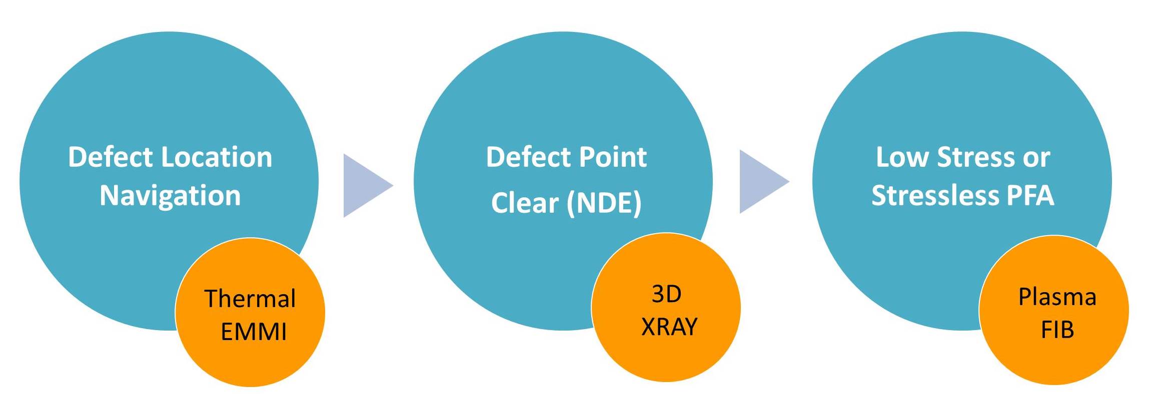
Step 1: Positioning
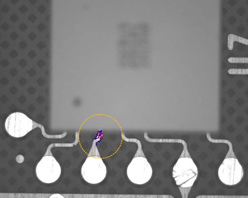
For WLCSP device having high-resistance after the reliability test, phase difference of Thermal EMMI hot spot is used to locate the failure position on a solder ball.
Step 2: Imaging
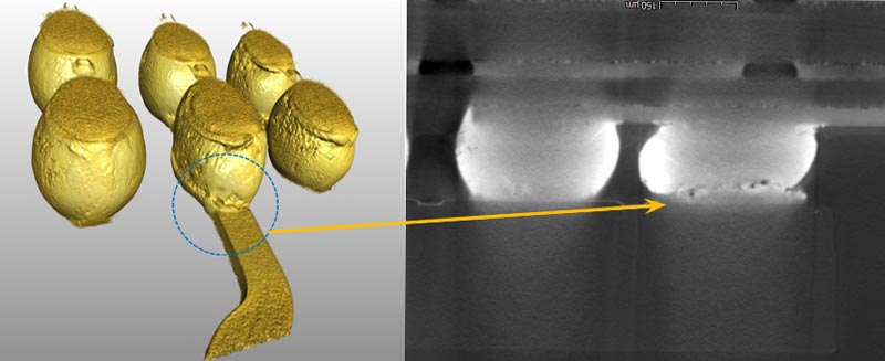
In order to not damage the “crime scene”, use 3D X-ray to scan 3D image ( lower left) and section image (lower right), therefore allowing the identification of the defective solder ball.
Step 3: Slicing
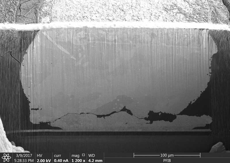
After identifying the relative position of the defect, the “crime scene” can now be removed using a low-stress Plasma FIB tool, with the failure section sliced out for cause analysis, verify that it is a Solder Ball Crack that causes the high-resistance anomaly and failure of the device .
We are more than glad to share our experiences with you. please call Ms.Chang at +886-3-579-9909 Ext. 6795 or email her at web_ise@istgroup.com