Issued Date:2024/5/7 Semi-Automated-Grinding-Polishing
Issued By:iST
Concerned about potential damage to valuable samples during manual grinding and polishing? Rest assured! iST’s semi-automated grinding and polishing technology ensures more accurate for high-quality sample preparation, effortlessly handling even the most challenging sample materials.
Semi-Automated-Grinding-Polishing

In today’s rapidly advancing technological era, advanced process packaging has been widely adopted in consumer electronics. However, because of its complex and precise structure, conducting destructive cross-section or horizontal polishing analysis often results in sample misalignment, uneven thickness, and even severe damage to IC structures, due to the difficulty in controlling traditional manual forces.
Through semi-automated grinding and polishing technology, these human-induced issues can be overcome, reducing the risk of sample damage and enhancing the accuracy of subsequent experiments. In this iST classroom, we will illustrate three major cases to provide you with a more reliable choice for sample preparation.
Semi-Automated-Grinding-Polishing
Semi-Automated-Grinding-Polishing
1. Semi-Automatic vs. Manual: Grinding Showdown!
Semi-automatic grinding / polishing, as the name suggests, automates part of the grinding and polishing process. By replacing hands with a robotic arm, samples can be prepared more accurately for subsequent placement on various microscopes, such as OM、SEM、FIB、TEM、AFM, etc., for failure or material analysis.
The difference in mechanical structure between the two, the traditional manual grinding / polishing machine is a single structure (Figure 1), while the semi-automatic grinding / polishing machine can be divided into two parts (Figure 2):
(1) Mechanical arm
(2) Grinding / polishing disc and control panel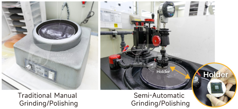
Figure 1: Traditional manual and semi-automatic grinding / polishing machine.
(Source: iST)The mechanical arm of the semi-automatic grinding / polishing system is also equipped with many knobs, which can adjust the angle and force of the downward pressure as needed. Therefore, each grinding / polishing process can be controlled very precisely, effectively removing excess layers (Delayer) from ICs. Subsequently, the system can not only measure thickness but also operate autonomously in an unmanned state through settings, improving sample abnormalities caused by human factors.
Traditional grinding / polishing relies on the experience and technique of personnel. In addition to requiring long training period, when facing large and long samples, the results of grinding often vary greatly. In contrast, beginners can easily get started with semi-automatic grinding machines.
However, traditional manual grinding / polishing is not completely defeated. Each grinding method has its own advantages, as shown in Table 1.
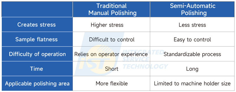
Table 1: Comparison of semi-automatic and traditional manual grinding / polishing machines (Source: iST)
2. Case Sharing of Semi-Automatic Grinding / Polishing
Currently, iST’s semi-automatic grinding / polishing machine can meet the preparation needs of various types of samples, such as package IC thinning, package solder joint grinding, IC backside thinning, and heat dissipation cover removal. Below, we will share three major cases of semi-automatic grinding / polishing used in iST’s sample preparation laboratory.
Case 1: Consistent Force and Level during Grinding/ Polishing
By using a semi-automatic grinding / polishing machine, the mechanical arm replaces manual grinding / polishing and takes advantage of standardization to ensure consistent force and horizontal line during each grinding / polishing process, effectively controlling the quality (as shown in Figure 3).
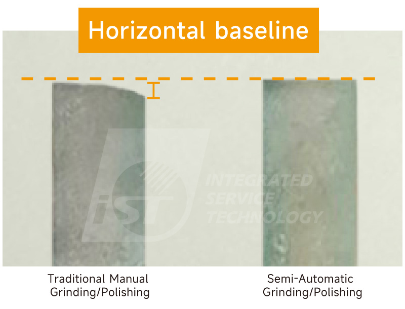
Figure 2: Semi-automatic grinding / polishing machine can effectively control the quality. (Source: iST)
Figure 3(a) shows a cross-section of the traditional grinding / polishing sample, where the vias are unevenly sized due to the tilted grinding / polishing angle. Figure 3(b) shows a cross-section of the semi-automatic grinding / polishing sample, which is flat due to the even downward pressure during the process, making it easy to control the horizontal line, resulting in consistent vias sizes.
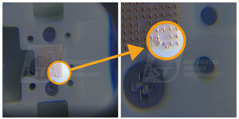
Figure 4: Semi-Automated-Grinding-Polishing testing can quickly rule out PCB issues and identify the root cause of the short circuit. (Source: iST)
(2) Passive Component Damage Results in Abnormal Resistance Values
Damage to passive components on the PCBA can result in abnormal resistance. Using conventional methods to customize ICT testing fixtures can take days to weeks. However, by employing ICT Semi-Automated-Grinding-Polishing testing, probes can accurately contact with test points on the components under test, enabling rapid measurement of passive components (resistors, capacitors). This approach swiftly identifies whether component values are abnormal.
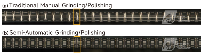
Figure 3: From the side view of the sample, it can be seen that after semi-automatic grinding / polishing, the sample is smoother than the sample treated with the traditional method. (Source: iST)
Case 2: Successfully Silicon Substrate Backside Thinning to Reveal All Anomalies
With the development of advanced processes, as chip structures are increasingly stacked, when samples experience electrical abnormalities, they often cannot be accurately localized due to the complex nature of chip circuits. At this time, a semi-automatic grinding / polishing machine can be used to uniformly thin the backside of the chip from 750um to only tens of microns (Figure 4), enhancing the ability of subsequent Infrared Ray Optical Microscope (IROM) to penetrate the substrate and observe anomalies more clearly (Figure 5).
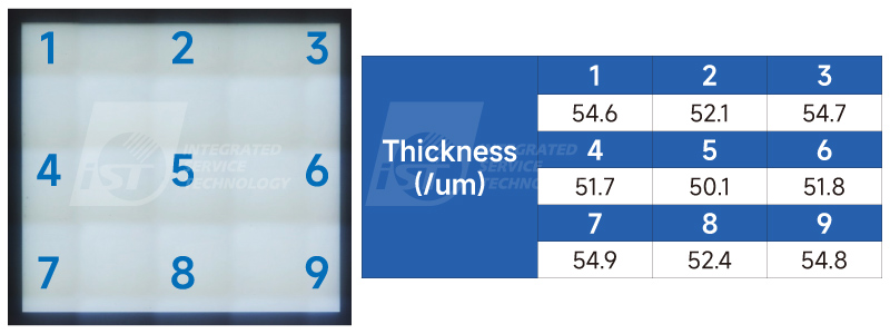
Figure 4: Using a semi-automatic grinding / polishing machine can stably and evenly thin the silicon substrate, and the thickness of the sample can be obtained at different positions using a thickness gauge. (Source: iST)
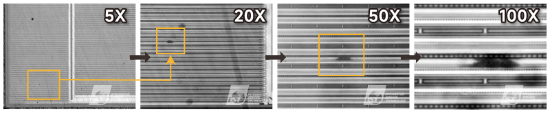
Figure 5: After thinning, the silicon substrate allows the subsequent IROM to observe the abnormal positions of the sample more clearly. (Source: iST)
Case 3: Achieving Excellent Grinding / Polishing Levels Even with Glass Materials
Taking CMOS image sensors as an example, due to the glass material in the surface layer of its structure and multiple layers of polymer materials in the stack, if chemical methods are used to remove the cover, the structure will inevitably be destroyed. At this time, by using the semi-automatic grinding / polishing machine, glass can be uniformly thinned, and subsequent DB-FIB and TEM experiments can obtain more accurate analysis (as shown in Figure 6).
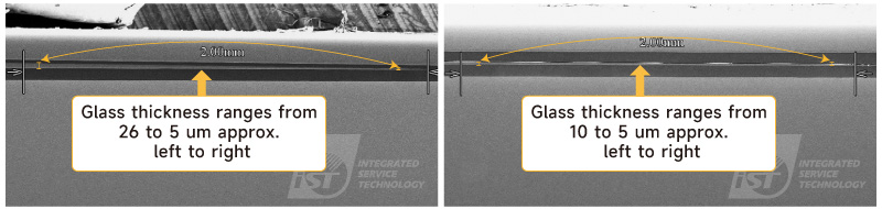
Figure 6: SEM images of the schematic structure of a CMOS image sensor. The left image depicts glass thinning using manual grinding / polishing machine, showing uneven thickness within a 2mm range when observed from the side. The right image illustrates glass thinning using a semi-automatic machine, resulting in more uniform thickness within a 2mm range, all falling within 10 um, facilitating subsequent failure analysis.
(Source: iST)
iST’s application of semi-automatic grinding / polishing technology enables a more efficient and precise sample preparation process. Through the cases shared in this session, we have explored the advantages of semi-automatic grinding / polishing in various application scenarios, aiming to assist you in obtaining more accurate results in subsequent analyses.
We appreciate the ongoing support from you all. If you would like to further understand the details, please feel free to contact Ms. Wang at +886-3-579-9909 ext. 6648 or via email web_pfa@istgroup.com ; marketing_tw@istgroup.com