Issued Date:2025/10/21 HAST PCB Fail
Issued By:iST
You might assume that the HAST is only verifying the IC, but often, the PCB is the first component to fail. In the AI, HPC, and advanced-packaging era, the PCB is no longer a mere supporting actor. Want to secure your yield? Don’t just look at the chip; start with the PCB.
HAST PCB Fail
In practice, engineers frequently see HAST (Highly Accelerated Stress Test) failures after mounting the IC to a PCB for bias-humidity stress. The core question then is: did the IC/module truly fail, or did the PCB fail first?
Since HAST testing requires the IC to be mounted onto a PCB, if the PCB’s insulation and stability are inadequate, it often fails sooner than the IC. This not only complicates the data interpretation but can also mislead engineers into thinking the IC is the source of the problem. This scenario—where the test vehicle fails before the product—is a persistent challenge in reliability verification.
The upcoming TPCA exhibition this year will focus on “Energy Efficient AI from Cloud to the Edge,” emphasizing the future direction of PCBs toward High-Density Interconnect (HDI), high-precision multi-layer routing, and high-frequency, low-loss materials. This is necessary to meet the industry’s demand for high-speed transmission, low energy consumption, and high reliability. Driven by the fervor for AI, HPC, and Co-Packaged Optics (CPO), the semiconductor supply chain’s emphasis on high-reliability PCB substrates has reached an unprecedented level. The PCB is no longer just a carrier for electronic components; it is a critical core component determining system performance and long-term reliability.
This iST Tech Classroom summarizes common PCB failure modes observed after HAST. We will provide practical prevention recommendations from the perspective of Layout Design and Process Optimization, helping you avoid costly detours in this era of high speed and high reliability.
HAST PCB Fail
HAST PCB Fail
iST observations have identified several abnormal PCB failure modes frequently encountered after HAST testing, including: Conductive Anodic Filament (CAF), Dendrite (Metallic Tree-like Crystal), Microcracks at interfaces, and Copper Migration (Cu Migration). We share case observations and prevention advice for each below.
1. CAF Case Observation and Prevention
CAF (Conductive Anodic Filament) is an electrochemical migration failure mode that can occur in PCBs under conditions of high humidity and bias voltage. Metal ions (typically copper ions) can migrate along the interface between the glass fiber and the resin, or through interface micro-cracks, gradually forming a filamentous conductive channel. If these filaments connect adjacent inner layer conductors or vias, it can lead to internal short circuits, insulation breakdown, or leakage.
During the PCB manufacturing stage, incomplete drying or poor resin/interface cleanliness can lead to a phenomenon known as Wicking: copper plating penetrates along the interface to the exterior of the substrate material. This copper penetration not only compromises dielectric isolation but also creates a potential path for subsequent CAF growth.
This article uses the schematic shown in IPC-A-600 as an example to illustrate the determination of Wicking and its impact on CAF risk, and further discusses prevention strategies in high-density design and process control.
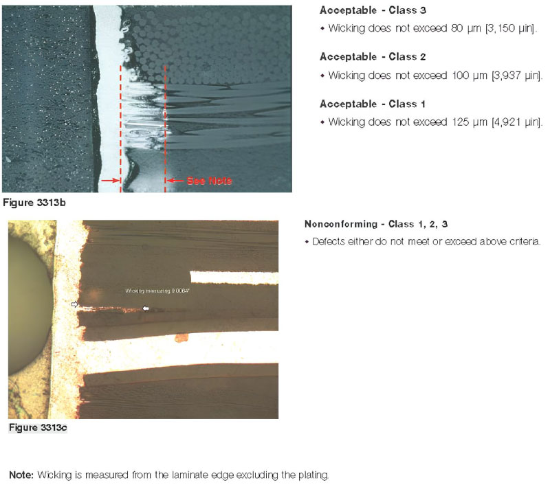
Figure 1: Schematic of Wicking in a plated through-hole cross-section
(Source:IPC-A-600)Due to the constraints of modern high-density designs (such as IC pitch of 0.3 mm or smaller), the spacing between traces and vias is difficult to increase. Although the IPC-A-600 standard allows acceptance up to Class 3 ≦ 80 µm, but this “standard value” is not equivalent to a “safe value” for reliability verification.
Under environments of high temperature, high humidity, and bias voltage, CAF or Wicking may still occur even if the design fully meets qualification. Therefore, the design and manufacturing teams must work together to jointly establish CAF and Wicking prevention benchmarks to reduce the probability of CAF occurrence. The following are iST’s recommendations for CAF prevention design and process countermeasures.
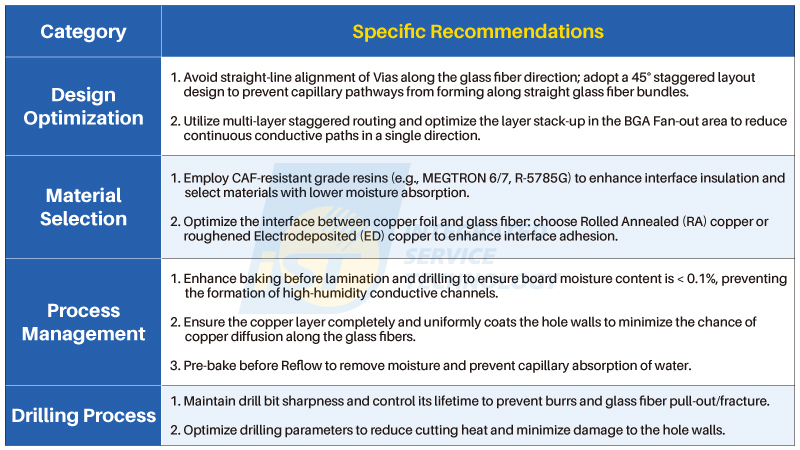
Table 1: CAF Prevention and Countermeasures
2. Dendrite Case Observation and Improvement
In HAST testing, if flux residue on the PCB or module surface is not properly cleaned, the residual salts or ionic contamination, combined with high temperature, high humidity, and bias voltage, will promote the migration of metal ions, forming a metallic, fern-like structure—this is called Dendrite.
As shown in the figure below, these dendritic structures typically extend outward from the edge of the solder pad and may eventually connect to an adjacent electrode, causing a surface short circuit. Dendrites are most likely to appear under BGA solder joints or in areas not protected by underfill or encapsulation.
Especially in lead-free soldering processes, the combination of residual salts in the flux with moisture, coupled with a bias voltage, provides the perfect conditions for metal ion migration. The result is that poor cleaning, high humidity, and bias voltage easily lead to the formation of metallic dendrites, causing conductive failure.
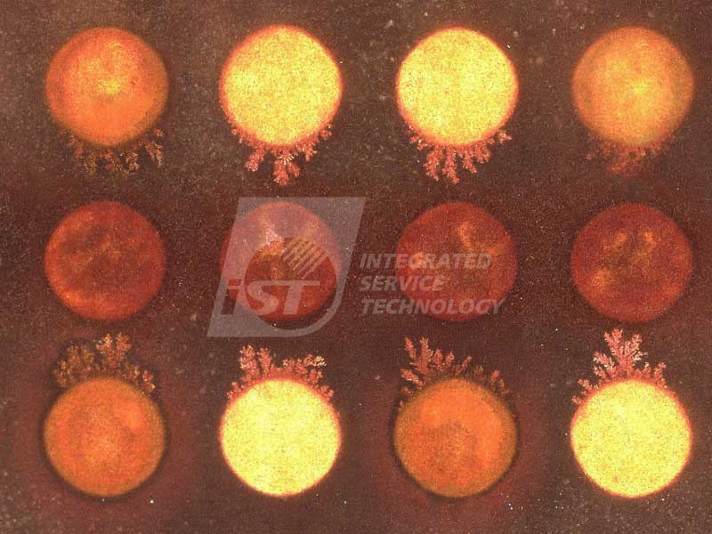
Figure 2: Dendrite formation creating a conductive path between solder pads.
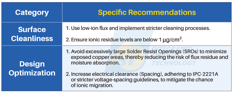
(Source: iST)Table 2: Dendrite Prevention and Countermeasures
3. Interface Microcracks and Metal Migration Case Observation and Improvement
(1) Interface Micro-crack
Scanning Electron Microscopy (SEM) sometimes reveals small cracks between the plating layer and the interface. Under HAST conditions, these cracks can lead to metal diffusion or copper penetration, causing conduction. These microcracks are often caused by residual chemicals from the desmear process that were not neutralized, or they may be stress cracks exacerbated by large differences in the Coefficient of Thermal Expansion (CTE) between materials during thermal cycling. To prevent such issues, iST recommends optimizing the lamination and Plated Through-Hole (PTH) process conditions and utilizing epoxy substrates with high heat resistance and low moisture absorption. Optimizing both process and material suppresses the formation of interface micro-cracks.
(2) Cu Migration
Under HAST conditions (high temperature, high humidity, and bias voltage), due to high water absorption in the board resin, interface contamination during the PTH process, or moisture absorption by the hole walls, metal ions can diffuse and penetrate within the inner layer traces or solder pad interfaces. This forms a conductive channel, and if the diffusion path overlaps with an adjacent conductor, it can cause a short circuit or insulation failure. This phenomenon is called Cu Migration (Copper Migration). Its mechanism is similar to CAF, but the diffusion path does not necessarily follow the glass fiber bundles; it can diffuse through the resin material itself. This failure mode is often seen in areas with dense inner layer routing, high moisture content, or insufficient PTH process control.
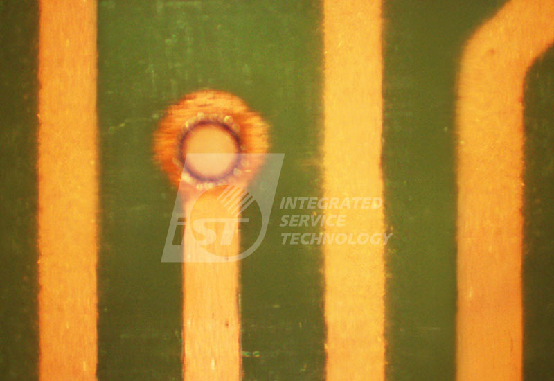
Figure 3: Cu Migration occurring between inner layer pads and traces.
(Source: iST)To prevent such issues, iST recommends strictly controlling the board moisture content (<0.1%), optimizing the drying and plasma cleaning processes before PTH, and avoiding overly dense inner layer conductor designs. Through a three-pronged approach involving design, process, and material management, Cu migration can be effectively suppressed, ensuring the PCB maintains stable insulation and reliability in high-humidity and high-voltage environments.
HAST testing is highly effective at simulating the stress placed on circuit boards in extreme environments. These failure phenomena are often related to multiple links, including material selection, design layout, drilling, and PTH processes, making it impossible to identify the root cause in a single stage. However, poor PCB design or lax process control can easily trigger micro-short circuit issues.HAST PCB Fail
iST’s one-stop service covering PCB design/manufacturing review, reliability verification, and failure analysis (such as cross-sectioning, SEM, EDS, and electrical tracing) can help you identify potential risks early, clarify the source of the problem, and provide concrete improvement recommendations, preventing the costly correction expenses that arise after mass production.HAST PCB Fail
For immediate access to the meticulously prepared chart, please email: marketing_tw@istgroup.com. If you’re interested in the micro-failure mechanisms of PCBs under HAST testing, please contact Ms. Lin at +886-3-579-9909 ext. 6480 | Email: web_rce@istgroup.com.