Issued Date:2025/9/9TGV Failure Analysis
Issued By:iST
TGV (Through-Glass Via) glass substrates, with their superior high-frequency and low-loss characteristics, are widely used in fields such as 5G, AIoT, and automotive radar, becoming a new option for advanced packaging. However, the industry often faces challenges in process yield, package mechanical strength, and material thermal mismatch (CTE mismatch) when introducing TGV technology. How can we identify the root causes of failures and improve yield?
TGV Failure Analysis
TGV Failure Analysis
TGV Failure Analysis
The semiconductor industry is undergoing a revolution in substrate materials! As applications such as AI, high-performance computing (HPC), and electric vehicles grow rapidly, the demand for low-loss, high-frequency characteristics and cost efficiency has increased focus on glass substrates for Through-Glass Vias (TGV) in advanced packaging. TGV is emerging as a promising technology in the AI revolution, with the potential to replace silicon-based interposers (Silicon Interposer).
Industry reports show that major companies like Intel, Samsung, Hana Technology, and Nippon Electric Glass (NEG) are investing in the development and pilot production of TGV, designing new packaging architectures for AI chips and high-frequency modules. Verified Market Reports forecasts the TGV market to grow from USD 1.2 billion in 2024 to USD 2.5 billion by 2033, with a compound annual growth rate (CAGR) of 9.5% from 2026 to 2033, highlighting its competitive potential.
What is TGV glass substrate technology? TGV is a process for creating “metal-filled through-glass via” on glass substrates. It involves drilling holes in a glass plate and filling them with conductive metal (such as copper), allowing electrical signals to pass through the glass. This creates high-speed channels, enabling fast, low-loss signal transmission between chips.
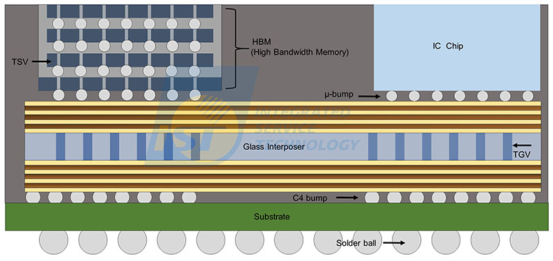
Figure 1: Schematic Diagram of TGV
(Source:iST)
Compared to silicon-based interposers, TGV technology offers key advantages in high-frequency transmission and excellent insulation, making it one of the crucial technologies for next-generation 2.5D and 3D advanced packaging. It is ideal for high-speed modules used in AI, 5G, and automotive radar. However, when introducing TGV technology, process yield, package mechanical strength, and material thermal mismatch pose significant bottlenecks that impact reliability validation and slow down mass production.
In this article, iST Classroom explains how we use iST’s and industry experience to identify the root cause of product failures through a four-step solution. We will also present a real-world case to illustrate the applications and potential risks of TGV technology.
1. The Two Major Challenges Facing TGV Development:
(1) Manufacturing Yield and Cost Challenges
1.Glass Drilling Issues: Currently, laser or chemical etching still face problems such as inconsistent hole shape and high surface roughness, which affect subsequent conductivity and the uniformity of metal filling.
2.Copper Filling and Diffusion Risks: Uneven filling leads to variations in hole resistance, and copper diffusion into the glass may cause insulation degradation and long-term failure.(2) Mechanical Strength and Packaging Stress
1.High Brittleness of Glass Substrates: While glass has high stiffness, it is highly brittle, making it susceptible to electrical anomalies caused by microcracks during processing, packaging, testing, or use.
2.Large Difference in CTE between Copper and Glass: Long-term thermal stress accumulation can lead to interface delamination.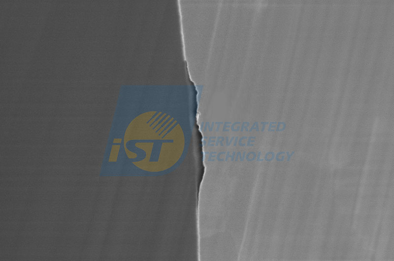
Figure 2: Delamination Anomalies between Copper and Glass in TGV.
(Source:iST)2. Time is Money: Four-Step Analysis to Quickly Identify Potential Anomalies
Next, we will openly share how iST’s Failure Analysis Laboratory identifies defects in TGV glass substrates. Through the following four steps, we effectively help customers quickly pinpoint potential defects and improve them. These steps are applicable to stages such as the initial TGV implementation, material selection, and pre-production reliability testing.
(1) Create the environment to trigger the manifestation of defects.
(2) Conduct non-destructive inspection to identify the defect areas in TGV and quickly locate the anomalies.
(3) Perform cross-sectional analysis of the defect to understand the actual failure phenomenon.
(4) Conduct microscopic material structure analysis to effectively mitigate potential risks.
Step 1: Create the environment to trigger the manifestation of potential defects.
Through accelerated aging reliability tests, such as HAST (Highly Accelerated Stress Test) and HTS (High Temperature Storage), the long-term stability of the TGV structure under high-temperature, high-humidity, and high-pressure conditions can be evaluated, triggering potential defects within the structure. This method simulates several years of lifespan in a short period, quickly inducing potential issues such as copper diffusion, glass interface delamination, or electrical conduction anomalies. iST can customize the test conditions (e.g., 85°C / 85%RH / 1000 hours) according to customer requirements and combine them with post-failure analysis to improve overall test effectiveness.
Step2: Conduct non-destructive inspection to identify the defect areas in TGV and quickly locate the anomalies.
When electrical leakage failures occur, hot spot analysis instruments (such as Thermal EMMI or OBIRCH) can be used to locate the defects. Additionally, using a high-resolution X-ray system, both 2D planar observation and 3D tomography scanning can be performed to quickly assess the electrical anomalies or copper via integrity of the TGV without damaging the sample. This technique can identify common void defects within the internal filling of TGV. We can also perform localized magnification analysis on high aspect ratio structures as a supporting basis for subsequent fine cross-sectional analysis.
Step 3 :Perform cross-sectional analysis of the defect to understand the actual failure phenomenon.
After defect localization, we can select the best preparation method for precise cross-sectional sample preparation based on the anomalies and the sample characteristics. This includes choosing from X-Section (Cross-sectional Grinding), CP (Cross-section Polisher), and Plasma FIB slicing techniques. (Read more: Among four major sectioning methodologies, which one is best for your sample?)
Step 4:Conduct microscopic material structure analysis to effectively mitigate potential risks.
After slicing, SEM or TEM can be used to observe the via interface condition, and EDS / EELS elemental analysis can confirm the copper diffusion path and concentration distribution. This step is crucial, especially when detecting trace copper diffusion within the glass, as it helps establish a comprehensive failure mechanism model. Additionally, EBSD analysis can be used to examine grain size/orientation, grain boundary characteristics, and residual stress, which aids in improving the process and enhancing reliability and electrical characteristics. (Read more: iST Tech Library Volume II-Unveiling the Hidden Threat in the TGV Process. How EBSD Tackles the Stress Issue)
3. TGV Case Study
In iST’s TGV anomaly analysis experience, the main cause of conductivity failure is often poor “glass hole quality” in the TGV process and uneven “copper filling” (typically electroplating or chemical plating). Since the tiny vias on the TGV substrate need to be fully and evenly filled with copper to ensure a stable conductive path, any anomalies in the glass etching process can lead to signal interruption. Additionally, improper electroplating parameters can result in voids, incomplete filling, or discontinuous columnar structures inside the vias, causing electrical anomalies and packaging failure.
In this case, 2D X-ray non-destructive analysis was employed to locate the defects, followed by precise cross-sectioning. SEM observations revealed uneven copper filling and voids, leading to some TGVs having conductivity failure or high resistance anomalies. After analysis, we optimized the copper plating conditions and adjusted the plating time, successfully allowing the customer to improve copper fill completeness and conductivity consistency, thereby enhancing overall yield.
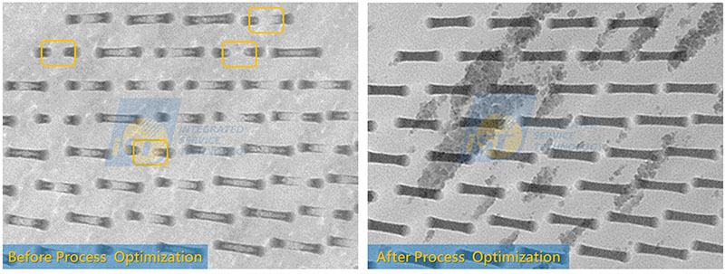
Figure 3: Observations from 2D X-ray reveal that the product originally had uneven copper filling, with vias that were not connected, indicating conductivity failure (the failed areas are marked with yellow circles in the left image). After optimizing and adjusting the copper plating conditions, the copper fill completeness was improved (right image).
(Source:iST)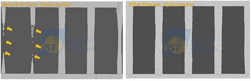
Figure 4: SEM images clearly show that after process optimization and adjustments, the copper fill completeness was successfully improved.
(Source:iST)
Despite the fact that silicon interposer technology remains the dominant solution in most applications due to its “mature process” and “excellent heat dissipation,” TGV glass substrates, with their low electrical impedance, high-frequency transmission, and exceptional insulation properties, have become one of the key materials in the semiconductor industry, driven by emerging trends such as AI accelerators, advanced communications, and millimeter-wave radar. With major global semiconductor companies actively investing, TGV glass substrates are expected to become a strategically significant “next-generation substrate” technology in the advanced packaging field. By using effective failure analysis methods to accelerate the improvement of TGV glass substrate reliability and process yield, the potential for early mass production of TGV can be significantly increased.
iST’s Verification and Analysis Laboratory has accumulated years of deep experience in TGV packaging reliability, establishing a rich case database for reference. From TGV via analysis and accelerated aging reliability tests to subsequent destructive high-resolution observations, the laboratory is equipped with a full range of testing equipment, including HAST, electrical hot spot analysis, 2D/3D X-ray, SEM, TEM, EDS, EELS, EBSD, XPS, SIMS, and more, offering a one-stop solution for TGV testing. This will help accelerate the development of TGV technology in various application fields, driving breakthroughs in high performance and high reliability.
This article shares our experience with all of you who have supported iST over the years. If you would like to learn more details, feel free to contact Mr. Lee at +886-3-579-9909 ext. 6741 or via email at web_ISE@istgroup.com ; marketing_tw@istgroup.com.