Issued Date:2022/3/24PFIB Delayer
Issued By:iST
Are you worried that the delayering process might damage your target area?
Are you concerned that uneven grinding of your sample could affect key observation points?

In general, sample preparation takes place before the physical analysis of IC defects, whereby the removal of package material is achieved by decap and delayering with laser and sample grinding to the target area, respectively.
With the evolution of Moore’s Law and the trend of miniaturization, however, the number of metal interconnect layers increases and 3D structure becomes sophisticated as the design advances. In addition, as the reduction of interlayer thickness and introduction of new materials sophisticate the structure of both interconnects and transistors, which makes the following failure analysis more challenging than before.
In particular, for advanced logic node and memory chips, it may be too risky to cover all hot spots on the same chip using grinding, what are the solutions?
In this iST classroom, we will share with you a powerful analysis tool, the Helios 5 PFIB UXe (PFIB). In addition to the small dual-beam FIB design for milling and capturing at the same time, it also supports large-area structure observation and enhances milling rate by over 20 times of the traditional dual-beam FIB to effectively shorten the analysis lead-time.
PFIB Delayer
- Equipped with the end-point monitoring mechanism and SEM real-time image support for precise judgment of delayering defect locations.
- Delayering results of large area with excellent uniformity can be provided through the gas-assisted plasma etching.
Table 1: Comparison of Traditional Grinding vs. PFIB Delayering
| Traditional Grinding | P-FIB Delayer | |
|---|---|---|
| Delayering range | Large | Relatively small (approx. 200μm*200μm) |
| Site-specific delayer | Difficult | Relatively easy through positioning from the machine |
| Damage range | Large (mechanical stress) | Controllable (ion beam damage) |
| Uniformity | Relatively low | Good (w/ gas-assisted etching) |
| Operator experience | Highly rely on operator experience | Easy to standardize into SOP |
Case 1: Overcoming poor uniformity of sample grinding with PFIB
As an extension of grinding delayer, PFIB can perform large area and excellent uniformity delayering of a specific area or layer through plasma etching with the manufacturer’s patented gas to fully present the target area of up to 200μm x 200μm (Figure 1).
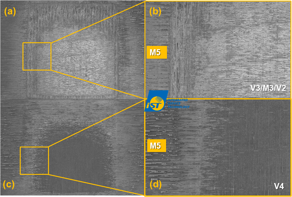
Figure 1 SEM imaging. Figure 1(a) shows the results without using PFIB gas-assisted etching. Figure 1(b) shows that the delayering uniformity is undesirable and cannot stay at the specific layer. By contrast, Figures 1(c) and 1(d) show the results of using PFIB gas-assisted etching with significant improvement.
Case 2: Overcoming accidental target area damage from over-delayering with PFIB
Precision endpoint judgement (Figure 2) is one of the PFIB functions for users to avoid accidental target damage caused by over-delayering. In addition, the passive voltage contrast (PVC) function can detect the location of defects with leakage or high resistance.
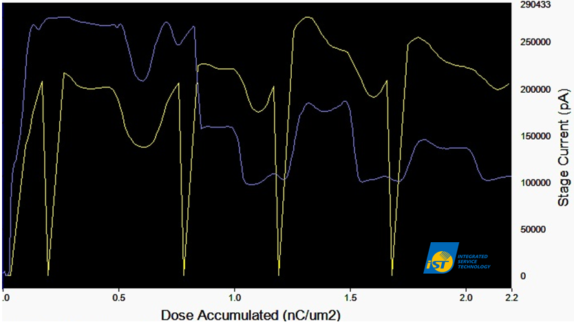
Figure 2 PFIB’s endpoint monitoring function. By detecting the tiny changes in stage current, the layer been removed can be traced and estimated precisely. This powerful function can help engineers to judge the endpoint of delayering more accurately to improve delayering accuracy.
Case 3: Large-area delayering of advanced processes chip
In the microstructure observation of advanced processes chip, traditional grinding will lead to the removal of multi-layers at the same time or poor-uniformity grinding because the layer thickness is too thin. The strength of PFIB enables complete and large-area delayering (Figure 3) with plasma etching.
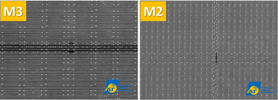
Figure 3 SEM image after PFIB delayering.
Currently, iST has developed experience in performing PFIB delayering analysis for 7nm and 5nm nodes on semiconductor components and 3D NAND flash. If you have doubts on the IC defect analysis or wish to find out more about PFIB analysis, you are welcome to contact Dr. Wei-Jui Lin at +886-3-579-9909 ext. 6166 or write to us at web_ma@istgroup.com.
Other services you may be interested in
PFIB Delayer