Issued Date:2026/6/30 EELS Applications
Issued By:iST

In our previous article《 EELS: The TEM Tool You Shouldn’t Overlook》, we introduced the structure and characteristics of EELS spectra. In this edition of “iST Materials Lecture,” we will delve deeper into the applications of EELS in material analysis, helping readers gain a clearer understanding of composition analysis techniques in TEM/STEM.
EELS Applications
We have a brief introduction of EELS, configuration and characteristics, in the previous article. Some applications of EELS in materials analysis will be discussed in article. These information may help readers to understand this TEM/STEM composition analysis technique more.
Current TEM/EELS analyses are performed by spectrum image technique in STEM mode as TEM/EDS analyses do. However, due to its high energy resolution, EELS can identify not only elements but also their chemical bonding states, such as carbons of coal coke, graphite, and diamond as well as silicon of silicon and silicon oxide [1]. Meanwhile, EELS is able to measure the thickness of the specimen [2 ~ 4]. Only a few TEM techniques can measure specimen thickness, and EELS is the only one can measure specimen thickness under the condition of analyzing directly. Other measuring techniques have to tilt the specimen to some adequate angles or adequate diffraction conditions [5 ~ 7], then calculate back to specimen thickness of being analyzed.
EELS Applications
EELS Applications
1. Characterization of elemental chemical state by EELS
Solid materials consist of countless atoms which aggregate together in specified spacings. Each atom can be divided into two regions: a nucleus at the center and electrons surrounding the nucleus. For general solid materials, the energy states of nuclei do not have detectable changes no matter what kind of atoms are near-by. We always neglect the change in nuclei in the field of science and engineering of materials. On the other hand, the distribution of electrons in both energy states and space changes when different atoms are bonded. All these changes are displayed in corresponding near edge fine structures (NEFS) of characteristic edges in EELS spectra.
Figure 1 shows three different Al L-edges, aluminum, alumina and aluminum nitride respectively. These fine structures in characteristic edges are unique correspondence as human fingerprints. So, the kind of the compound can be identified by its characteristics edge.
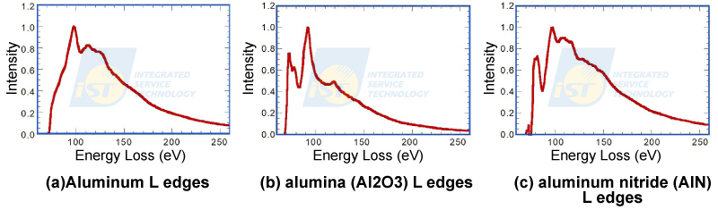
Figure 1. Background subtracted Al L edges.
(a) Aluminum L edges, (b) alumina (Al2O3) L edges, (c) aluminum nitride (AlN) L edges.
(Source: iST)All TEM laboratories should build their own data base of EELS characteristic edges of materials they use routinely to characterize elements in materials efficiently. It is not a hard job to build data base of EELS characteristic edges in semiconductor industry, since limit elements are used in this field. But it is not an easy job for the field of science and engineering of nano materials, since so many elements and allotropes are involved. These make some standard samples be not available easily. In this case, some characteristic edges built in famous international TEM laboratories can be referred to as standards firstly, then further improvement must be taken gradually.
2. EELS mapping – Distribution of an element of different chemical state
The change in bonding energy due to valence change of elements falls in the range of 1 ~ 10 eV. The best energy resolution of EDS, which is used most widely in TEM composition analysis, is about 126 eV. So, all energy peaks of allotropes of elements are identical. For FEG TEMs, the energy resolution of EELS is always better than 1.0 eV, so EELS can distinguish the chemical bonding state of elements. The chemical bonding state of elements can be uniquely identified by their threshold energies and near edge fine structures in EELS spectra.
When more than one valance for an element is found in the EELS spectra of an analyzed region, it is possible to map them seperately by setting adequate energy windows. Figure 2 shows a typical example. Figure 2(a) is a TEM BF image of a Si-based semiconductor device, Figure 2(b) is a Si map showing positions of Si-substrate and poly silicon, Figure 2(c) is a Si4+ map showing positions of silicon-oxide, and Figure 2(d) is a O2- map matching the position of Si4+shown in Figure 2(c).
iST’s current STEM/EELS analysis capabilities has been able to map silicon in silicon substrates & poly silicon, silicon dioxide, silicon nitride, and cobalt disilicide respectively.
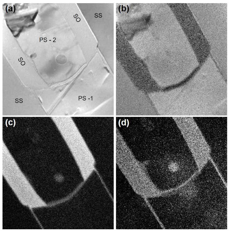
Figure 2. TEM BF image of a semiconductor device and corresponding EELS maps. (a) TEM BF image, (b) Si (of Si) map, (c) Si4+ (of SiO2) map, (d) O map. (Ref: [8, 9])
(Source: iST)3. Measurement of TEM specimen thickness
Conventional TEM images have nanometer to atomic resolution in xy plane, while the resolution in z direction (along electron beam path) is rarely mentioned. Most of TEM analyses can be performed without knowing TEM specimen thickness. But some special analyses for material systems, such as nano-precipitates density in aluminum alloys and dislocation density in GaN epitaxy, the volume density of them can be calculated only when the thickness of the analyzed region is known. Among several TEM analytic techniques for measuring specimen thickness, EELS is the only technique that can measure the specimen thickness right at the condition of imaging.
The thickness of the analyzed region can be estimated by the intensity ratio of the low loss peak to the zero loss peak as well as the number of low loss peaks, as shown in Figure 3. There is a zero loss peak only when the electron beam enter the EELS spectrometer without passing through the specimen (Figure 3(a)), a small low loss peak shows up when the electron beam goes into the thin region of the specimen (Figure 3(b)). The intensity of the loss peak increases with the specimen thickness (Figure 3(c)). As the specimen thickness increases more, the second and the third low loss peaks emerges subsequently ((Figure 3(d) and (Figure 3(e)).
When the electron beam enters the specimen in the region A as marked in Figure 3, a few of high energy electrons are single inelastically scattered. Some high energy electrons suffer one or two inelastic scattering in the region B, and some high energy electrons are inelastically scattered more than twice in the region C. The inelastic scattering in region B and region C is called plural (or multiple) inelastic scattering. For quantitative analysis, EELS analysis should be performed in the region A to keep the accuracy as good as possible.
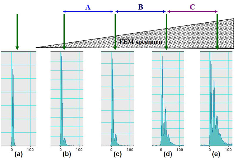
Figure 3. Relationship of the intensity ratio of zero loss peak (ZLP) and low loss peak (LLP) with the specimen thickness.
(a) a ZLP (no specimen), (b) a ZLP + a LLP (very thin specimen region),
(c) a ZLP + a LLP (thin specimen region), (d) a ZLP + 2 LLPs (thick specimen region),
(e) a ZLP + 3 LLPs (very thick specimen region). (Ref: [9])
(Source: iST)Equation (1) is used to analyze the specimen thickness in EELS analyses.
Io = It exp(-t/λ) ………………..(1a)
t = λ ln (It / Io) ………………..(1b)
Here, Io is the integrated intensity of the zero loss peak and It is the integrated intensity of the whole spectrum, t is the specimen thickness, λ is the average mean-free path of inelastic scattering of the analyzed specimen. Generally, Io is integrated from -5.0 eV to 5.0 eV, and It is integrated from -5.0 eV to 600.0 eV. The λ value of a specified material is affected by both the TEM operation voltage and collection angle of EELS. λ increases with the TEM operation voltage.
Graphene, also known as single-layer graphite, is a two-dimension material with very good physical properties. The thickness of a single layer of graphite is 0.34 nm. Currently, single layer of graphene is hard to be manufactured, and those graphene with thickness less than 10 nm are generally accepted.
The TEM BF image shown in Figure 4 displays that graphene is supported by holy carbon film. Three positions marked on the image, position ①; is carbon film only, position ② is graphene only, and position ③ is carbon film and graphene. The total acquisition time is same, 0.5 s, for all them. The y-axis of Figure 4 is in log scale, and the intensity of zero loss peaks of these three EELS spectra are nearly same, while intensities of low loss peaks are ③ >② > ①. Specimen thickness of t1, t2, t3 are calculated to be 0.138 λ、0.299 λ、and 0.438 λ respectively by DigitalMicrograph. The value of of carbon is 20 nm from tabular data. So, the thickness of carbon film and graphene is ~ 2.8 nm and ~ 6.0 nm respectively.
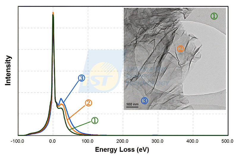
Figure 4. TEM specimen thickness measurement EELS.
Region ① is carbon film of Cu grid (green-line spectrum),
region ② is graphene,
region ③; is “carbon film + graphene”.
(Source: iST)4. Separate the wheat from the chaff -EELS Energy Filtered Image
When high energy electrons go through the specimen, some of them interact with electrons in the specimen inelastically and lose a few of energy. TEM objective lenses deflect these electrons of less energy more, so electrons of zero loss focus on the image plane and form the signals, while those electrons losing some energies focus in front of the image plane then diverge on the image plane and form the background in the image, as described by rays in the schematic diagram (Figure 5). Green lines represent the paths of zero-loss electrons and light green lines represent paths of electrons of losing energy. This phenomenon is named to be chromatic aberration in TEM imaging [3]. Effect of chromatic aberration increases with the specimen thickness.
The distribution of electrons of various energies is random and unable to be separated in traditional TEMs. They will be arranged linearly by being defected two times when they enter the EELS spectrometer. An adjustable slit , working as a energy window, is installed in the path of linearly arranged electrons to block electrons suffering energy loss to enter the image detector as illustrated in Figure 6. In this process, energy deviation of electrons used to form the final image are limited in a range ΔE(2 ~ 4 eV). The effect of chromatic aberration will be minimized, and image of thick region can be clear, an example is given in Figure 7.
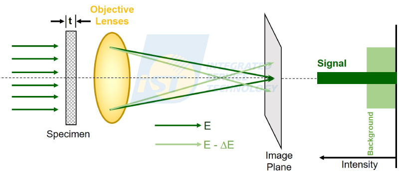
Figure 5. A schematic diagram displays the formation mechanism of background in TEM images by chromatic aberration effect.
Electrons focus in front of the image plane diverge on the image plane and become blurred background.
(Source: iST)![EELS Applications When high energy electrons go through the specimen, some of them interact with electrons in the specimen inelastically and lose a few of energy. TEM objective lenses deflect these electrons of less energy more, so electrons of zero loss focus on the image plane and form the signals, while those electrons losing some energies focus in front of the image plane then diverge on the image plane and form the background in the image, as described by rays in the schematic diagram (Figure 5). Green lines represent the paths of zero-loss electrons and light green lines represent paths of electrons of losing energy. This phenomenon is named to be chromatic aberration in TEM imaging [3]. Effect of chromatic aberration increases with the specimen thickness. The distribution of electrons of various energies is random and unable to be separated in traditional TEMs. They will be arranged linearly by being defected two times when they enter the EELS spectrometer. An adjustable slit , working as a energy window, is installed in the path of linearly arranged electrons to block electrons suffering energy loss to enter the image detector as illustrated in Figure 6. In this process, energy deviation of electrons used to form the final image are limited in a range E(2 ~ 4 eV). The effect of chromatic aberration will be minimized, and image of thick region can be clear, an example is given in Figure 7.](https://www.istgroup.com/en/wp-content/uploads/2026/06/tech_20260707-EELS-06.jpg)
Figure 6. Schematical diagram shows the relationship between EELS spectra and the effect of chromatic aberration in TEM images.
(a)Electrons in zero loss peak form the signal (focused image), and electrons of losing partial energy form the background (unfocused image).
(b) The background of image is reduced when electrons of losing partial energy are filtered off by the inserted slit.
(Source: iST)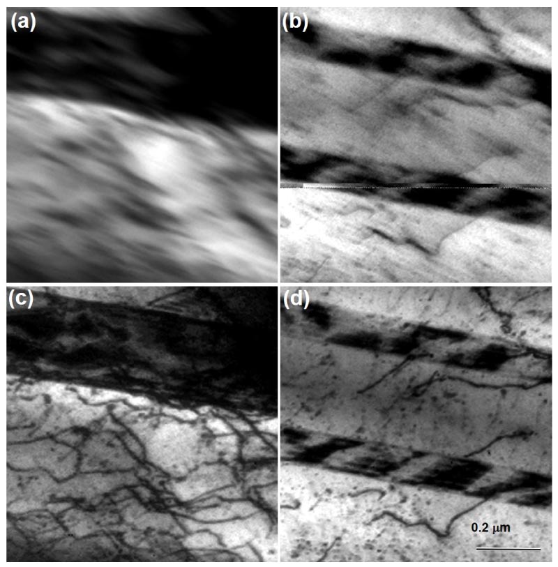
Figure 7. TEM BF images and corresponding EELS energy filtered images of thick specimens.
(a) and (b) are unfiltered TEM BF images, (c) and (d) are filtered TEM BF images.
(a) and (c) t = 208 nm, (b) and (d) t = 88 nm. (Ref: [9])
(Source: iST)
EELS can not only characterize elements but also identify their valences by means of its superior energy resolution. Besides characterizing the existence of allotropes by spectrum analysis, EELS can identify their distribution by mapping.
Meanwhile, EELS is able to measure the specimen thickness in order to know the volume analyzed. So, precipitates and crystal defects can be analyzed quantitatively. By employing the technique of energy filtered imaging, EELS can prevent inelastic scattered electrons to contribute to the final image, so effect of chromatic aberration can be minimized. This makes the images of thick regions as clear as those of thin regions.
The analysis technique of STEM/EELS in iST has been established and developed to a mature stage. Elemental maps of silicon in the Si substrate and poly silicon, silicon dioxide, silicon nitride, and cobalt silicide in the metal-oxide-semiconductor (MOS) structure can be mapped separately. Whether for material identification or structural anomaly diagnostics, we provide the most intuitive and reliable data support, serving as the strongest backbone on your R&D journey. For more information, contact Ms. Chen: +886-3-579-9909 Ext. 1065 | Email: marketing_tw@istgroup.com
References:
[1] https://www.globalsino.com/EM/page4709.html
[2] R. F. Egerton, “Electron Energy-Loss Spectroscopy in the Electron Microscope, 2nd edition (1996).
[3] D. B. Williams and C. B. Carter, in Transmission Electron Microscopy, (2009).
[4] https://eels.info/how/quantification/assess-sample-thickness
[5] https://www.globalsino.com/EM/page4622.html
[6] https://appmicro.springeropen.com/articles/10.1186/s42649-020-00029-4
[7] https://www.researchgate.net/publication/16701730_Methods_for_specimen_ thickness_determination_in_electron_microscopy
[8] J. S. Bow et. al. Proc. ISTFA, 101-105 (2002).
[9] 鮑忠興和劉思謙,近代穿透式電子顯微鏡實務,第二版,第五章, (2019)