Issued Date:2025/12/16 SiPh CPO
Issued By:iST
From Electrical Limits to Optical Challenges, Who Will Lead the Next Wave of AI Infrastructure? As global AI leaders double down on next-generation compute, a pivotal question dominates the industry: why has silicon photonics—despite massive investment and engineering talent—still not crossed the threshold into true mass production?
SiPh CPO
SiPh CPO
SiPh CPO
By 2025, the demand for high-speed AI computation has reached unprecedented levels. Across the global AI supply chain, one reality is undeniable: electronic interconnects have pushed against their physical bandwidth limits. Optoelectronic integration is no longer an alternative—it is inevitable. At the forefront of this transition stand two technologies: Silicon Photonics (SiPh) and Co-Packaged Optics (CPO).
Momentum is building worldwide. NVIDIA has committed to silicon-photonics adoption; Broadcom is accelerating next-generation Ethernet platforms; TSMC is advancing its COUPE photonic-engine architecture. Taiwan has placed silicon photonics within its “Ten New AI Infrastructure Projects,” targeting supply-chain independence by 2028. The Ministry of Economic Affairs has allocated NT$2.9 billion to photonics R&D to position Kaohsiung as a global hub.
Even with some of the world’s strongest engineering teams and substantial government backing, moving silicon photonics into true mass production is anything but straightforward. Once photonic integrated circuits (PICs) are brought onto the chip, the entire verification flow shifts abruptly from familiar electrical-IC (EIC) issues to photonic ones. Many R&D teams find that, even after they have solved the architectural design, they are still blocked by optical characterization: silicon-photonics test is simply too slow to keep up with design cycles; optical loss cannot be accurately localized or quantified; and irreversible post-packaging failures continue to weigh on yield.
In our earlier article, we outlined five major R&D challenges in silicon-photonics development and the corresponding mitigation strategies (Read more: Why Silicon Photonics Development So Hard?Verification is the Key). In this iST Classroom edition, we take a deeper look at the core obstacles standing in the way of mass production, and show how iST helps engineers accelerate CPO development and move more confidently toward volume manufacturing.
1. Why Silicon Photonics Sits at the Core of CPO?
Silicon photonics brings a unique advantage to CPO: its core building blocks—waveguides, modulators, demultiplexers, couplers, and high-speed photodiodes—can all be manufactured in standard CMOS fabs (Read more: “Optical” Breakthrough: Silicon Photonics Chips Ready to Launch).
This unlocks true scalability, enabling PICs to be co-packaged or even monolithically integrated with cutting-edge electronic ICs.SiPh CPO
By placing optical and electrical domains on the same substrate, CPO architectures break through the long-standing limits of copper interconnects. Systems gain wider bandwidth, lower power, faster signaling, and dramatically better signal integrity—while avoiding skin-effect loss, crosstalk, and insertion-loss escalation. Energy per bit can fall from 15–25 pJ/bit to as low as 1–3 pJ/bit, easing the thermal burden that constrains next-generation AI platforms.
2. Mass Production Is Still Out of Reach—Three Verification Bottlenecks Remain
Despite its advantages, silicon photonics introduces a new physics domain unfamiliar to many electronic-circuit engineers. Across the industry, iST observes three recurring barriers that consistently slow mass-production readiness.
(1)Optical-Test Throughput is Far too Slow
Optical characterization—IL, PDL, responsivity, spectral response—requires full wavelength sweeps and repeated alignment for every die. Unlike electrical probing, there is no instant “plug-and-test.” These constraints make optical test dramatically slower, hindering design turnaround and delaying production ramp for high-speed SerDes and AI compute engines.
(2)Optical Loss Cannot be Directly Seen—Only Inferred
Conventional OWAT (Optical Wafer Acceptance Test) tools rely on reflectometry and spectral signatures. They can indicate degradation but cannot localize the loss mechanism or quantify its spatial origin.
As a result, design teams see performance dropping but cannot tell whether loss is coming from a coupler, waveguide transition, modulator junction, or post-bond interface. This lack of visibility causes repeated design-loop stalls and yield-learning delays.
What makes the challenge even greater is that optical signals in PICs are far more sensitive than electrical ones—and the factors contributing to optical loss are far more diverse and complex. Loss is not only difficult to predict; it is even harder to localize using traditional optical-measurement methods.
Because most applications that rely on silicon photonics are tied to high-speed interfaces and AI compute—such as SerDes drivers, TIAs, modulators, and control logic—the accompanying electronic ICs (EICs) often use advanced nodes such as 5 nm or 3 nm, where the cost per die is extremely high. PICs, by contrast, are typically fabricated using mature-node processes and are therefore far less expensive.
If optical-loss issues are discovered only at the heterogeneous-integration stage—when the PIC and EIC have already been bonded into a CPO module—the entire EIC becomes unrecoverable, and the full module must be scrapped. The financial loss multiplies quickly, making this one of the most cost-intensive failure modes in the industry.
For this reason, PIC dies must be accurately screened at the wafer stage, before ever entering the bonding or packaging flow.
Given these risks, PIC dies are often forced into 100% inspection to avoid discovering loss issues only after PIC–EIC bonding. However, full inspection is both time-consuming and costly, and still fails to fundamentally improve design-iteration efficiency during the mass-production phase.
These measurement limitations represent one of the most persistent—and most stubborn—bottlenecks preventing silicon photonics from moving beyond technological breakthroughs into true large-scale manufacturing.
(3)Latent Thermal Hotspots Drive Post-Packaging Failures
Because silicon-photonics components are highly integrated and place optical and electrical domains in extremely close proximity, localized thermal hotspots often develop inside the module. What makes this even more challenging is that these subtle heat sources are invisible to the naked eye and cannot be detected through traditional electrical measurements.SiPh CPO
Engineers typically notice only the symptoms—such as IL drift, degraded photodiode responsivity, or worsening BER—without being able to directly identify the location, magnitude, or root cause of the thermal source.
If these issues are not detected and localized early at the wafer or die stage, they can later manifest—after packaging or during system operation—as waveguide drift, increased optical loss, thermo-optic imbalance, or even premature device aging.
Once this happens, the entire module often becomes non-repairable and must be scrapped, significantly reducing the yield of CPO and optical-engine products.
3. iST × Enlitech: A New Evidence-Driven Solution for Silicon-Photonics Verification
To close these long-standing gaps, iST has partnered with Enlitech to create a unified testing platform that spans photonic components, wafers, dies, and full CPO modules.
The collaboration combines iST’s deep electrical-test and reliability expertise with Enlitech’s advanced photonics measurement technology. The result is a complete, wafer-to-module verification workflow designed specifically for silicon-photonics development.
(1) From Inference to Evidence: Spatially Resolved IL Mapping
Night Jar™ transforms optical-wafer testing from trend-level inference into evidence-driven diagnosis. The system integrates spatial IL mapping, localized loss-site identification, quantified IL values for every photonic structure, as well as high-resolution leakage imagery and loss-distribution maps.
With these capabilities, engineers can finally address questions that traditional OWAT has long been unable to answer—such as which die is anomalous, which waveguide or coupler is leaking light, and precisely how much propagation loss occurs at each location. Night Jar™ offers the diagnostic resolution required for fast design closure—something no conventional loss meter or reflectometry tool can deliver.
Figure 1. Illustration of a traditional OWAT optical measurement. This method provides only the total insertion loss and offers no insight into leakage location or the precise magnitude of optical loss.
(Source: iST)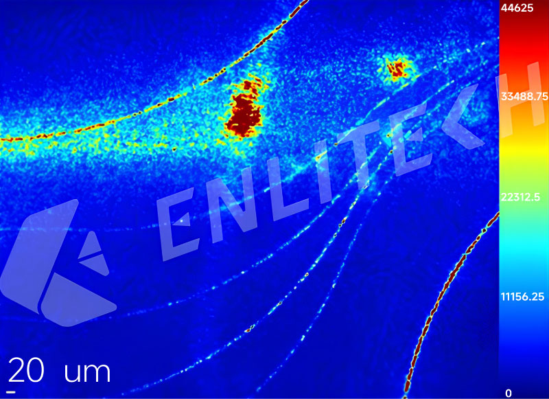
Figure 2: Night Jar™ enables users to directly see where optical loss occurs—revealing not only the loss magnitude but also the exact structure from which light leaks or dissipates.
This visibility is critical for failure analysis and design debugging.
(Source: Enlitech)(2) High-Speed Characterization with Precision Alignment
Night Jar™ captures IL-distribution frames at up to one region per second, more than doubling throughput vs. mainstream optical tools. Its 0.2-nm alignment precision ensures exceptional measurement repeatability—a critical factor for yield learning, process tuning, design-parameter extraction, reliability correlation.
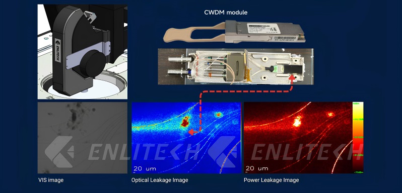
Figure 3: Real-world measurement capability of Enlitech’s Night Jar™ on commercially available silicon-photonics optical modules.
(Source: Enlitech)(3) Thermal–optical correlation reveals hidden risks
By combining IL Mapping with optical–thermal imaging, Night Jar™ uncovers hotspots that traditional tests cannot detect. Engineers can identify thermal drift in waveguides, localized overheating near modulators, laser-source thermal accumulation, PD temperature-induced instability. Detecting these risks at the wafer stage prevents costly module scrap.
(4) Enabling deep-level physical and structural analysis
Once loss mechanisms are localized, engineers can conduct targeted PFA and MA using:
SEM、Dual-Beam FIB、Plasma FIB、TEM、X-ray、SIMS .This reveals nanoscale defects or material variations within waveguides, couplers, modulators, or PD structures—accelerating both design refinement and process optimization.(5) CPO reliability qualification anchored on IL variation
Completed CPO modules, e.g. COUPE (Compact Universal Photonic Engine) then enter full reliability testing, including Temperature Cycling Test (TCT), HAST and humidity stress, Vibration, Particle contamination.
IL variation serves as the primary qualification metric, ensuring modules meet the stringent requirements of hyperscale data centers and AI infrastructure providers. Data-driven analysis allows engineers to quantify risks and make precise design and process decisions.
To cross the final mile from prototype to mass production, silicon-photonics platforms need more than strong designs—they need fast, evidence-based verification that exposes failures early, localizes defects precisely, and shortens iteration cycles.
From substrate and socket design, optical/electrical characterization, and reliability qualification to failure analysis and structural diagnostics, a seamless end-to-end workflow is the foundation of successful CPO deployment.
When the entire validation pipeline becomes smoother,the optical era arrives faster.
Interested in receiving the “iST Silicon Photonics Solutions Overview”?
Reply to this email now to connect with us! We will send you a detailed chart for your reference, helping you break through CPO R&D bottlenecks together!
For inquiries, please contact Ms. Skylar Chen at +886-3-5799909 ext. 8926│Email: ist_siph@istgroup.com ; marketing_tw@istgroup.com