Issued Date:2025/8/21 EBSD TGV
Issued By:iST
In TGV process, even minor variations in grain orientation and stress distribution often determine product reliability. This is precisely where EBSD excels
EBSD TGV
With the rapid advancement of advanced packaging technologies, Through-Glass Via (TGV) is increasingly emerging as a key interconnect solution for chips. According to reports, Taiwan’s Industrial Technology Research Institute (ITRI), supported by the Department of Industrial Technology (DOIT), has successfully developed a fully wet panel-level packaging system that improved the aspect ratio (AR) of 12-inch glass substrates from AR 10 to AR 15, breaking through traditional TGV process limits and significantly reducing manufacturing costs.
In this context, examining the crystalline structure using Electron Backscatter Diffraction (EBSD) becomes particularly crucial. EBSD enables in-depth analysis of grain orientation, grain boundary characteristics, and residual stress—key microstructural features that can help optimize process quality and enhance product reliability.
In the previous episode of iST Tech Library, we introduced the basics of EBSD, including how it interprets crystal orientations from electron diffraction patterns. If you’re not yet familiar with these concepts, we recommend reading that introduction first for a more complete understanding. (Read more: How to Understand Crystal Structures? EBSD Reveals the Secrets Inside Materials).
In this issue, we focus on EBSD’s practical role in TGV process—from grain size and boundary control, residual stresses analysis, to failure localization and quality management—revealing how EBSD helps overcome reliability challenges in advanced packaging.
EBSD TGV
EBSD TGV
With the rapid development of 2.5D/3D ICs, high-density interconnect (HDI), and glass substrate technologies, Through-Glass Via (TGV) shows great potential for applications in high-frequency, high-speed communication and computing chips. However, the metallization and thermal processing steps involved in the TGV process can lead to issues such as uneven grain orientation, unstable grain boundary structures, and residual stress—all of which may negatively impact reliability.
EBSD offers a microscopic analysis method capable of effectively observing and resolving these process-related challenges. Based on recent EBSD research, this article introduces how EBSD can be used in the TGV process to observe and evaluate grain size, grain boundary characteristics, and stress distribution, and explores how it can assist engineers in improving the quality and reliability of TGV structures.
1. EBSD Applications in TGV Process
1.1 Grain Size and Boundary Characteristics
Using EBSD data, one can calculate and statistically analyze grain size distribution and the proportion of high-angle grain boundaries (HAGBs).
According to a 2024 study by Chang et al. (J. Mater. Res. Technol), a multi-step electroplating process—especially with lower initial current density—can effectively control grain growth and improve microstructure. EBSD analysis showed this approach increased the proportion of HAGBs and twin boundaries (TBs) (Figures 1 & 2), which helps enhance the mechanical strength and ductility of electroplated copper and may also stabilize its electrical performance.
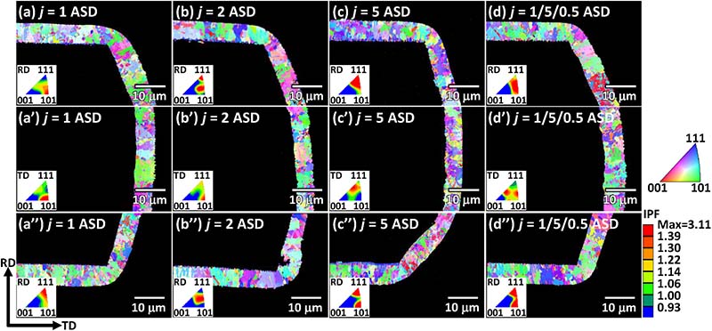
Figure 1. IPF maps of TGV copper regions under different plating conditions.
(Chang et al., 2024, J. Mater. Res. Technol.)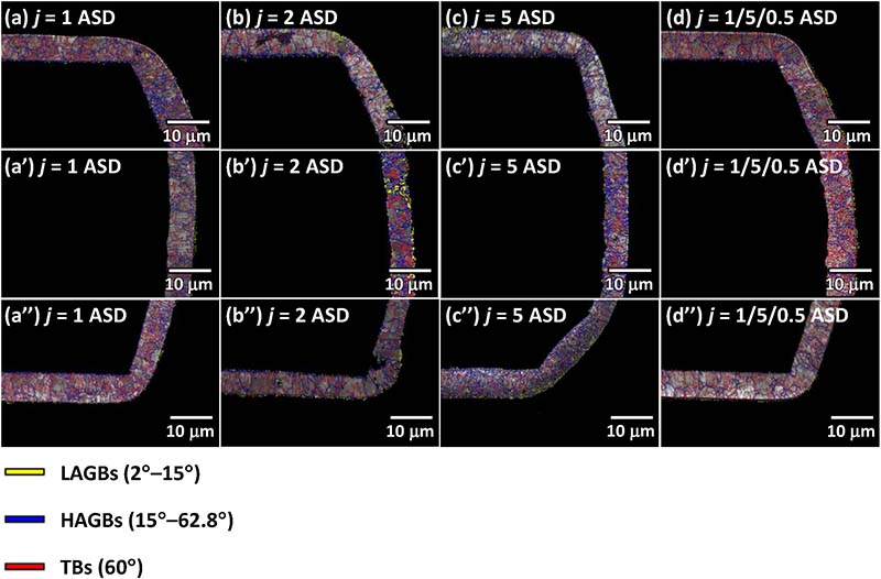
Figure 2. Comparison of grain-boundary–type fractions under varying plating parameters.
(Chang et al., 2024, J. Mater. Res. Technol.)In contrast, single-step electroplating tends to result in uneven grain sizes, which may lead to stress concentration. Although multi-step plating slightly reduces overall strength, it significantly improves ductility, helping to mitigate packaging stress and improve TGV copper reliability overall (Figure 3).
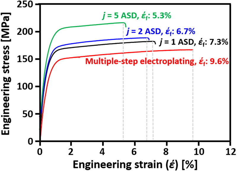
Figure 3. Stress–strain curves for Cu-plated samples under different plating regimes.
(Chang et al., 2024, J. Mater. Res. Technol.)1.2 Grain Orientation and Stress Correlation
EBSD can generate inverse pole figure (IPF) maps of electroplated copper in TGVs to analyze the relationship between crystal orientation and micro-scale stress.
According to Wang et al. (2024, J. Alloys Compd), EBSD and XRD were used to analyze the microstructural changes of copper films at different annealing temperatures. As annealing temperature increased, residual stress in the copper changed from -70 MPa (compressive) to around +15 MPa (tensile) (Table 1). EBSD results showed that annealing promoted static recrystallization, increased HAGB proportion, and refined grain size (Figure 4).
Table 1. Residual stress in TGV Cu films after annealing at various temperatures.
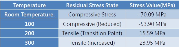
(Wang et al., 2024, J. Alloys Compd.)
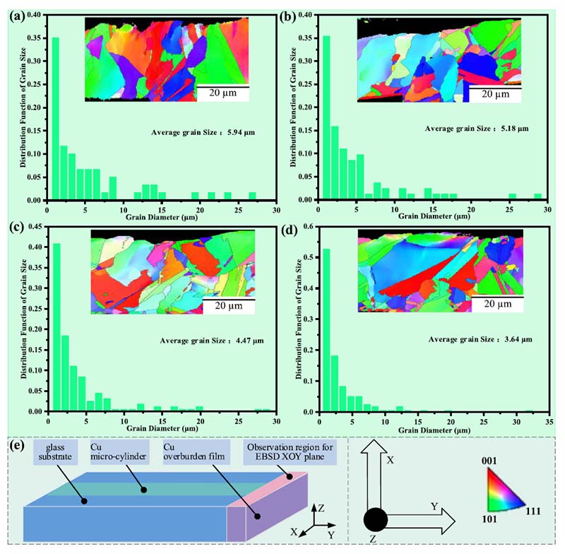
Figure 4. Grain-size and orientation distributions of the Cu overburden film at different annealing temperatures.
(Wang et al., 2024, J. Alloys Compd.)They also found that samples with high residual stress tended to show a (001) preferred orientation, while low-stress samples shifted to (111) orientation—considered more stable due to easy slip in FCC structures. Kernel Average Misorientation (KAM) analysis (Figure 5) revealed that internal strain decreased significantly between 100°C–200°C, suggesting effective stress relief via recrystallization. At 300°C, however, local strain increased again, indicating renewed stress buildup.
Thus, changes in grain orientation can serve as indirect indicators of residual stress levels. Continuous EBSD monitoring of orientation and dislocation density helps evaluate whether micro-stress is being effectively mitigated during electroplating and annealing.
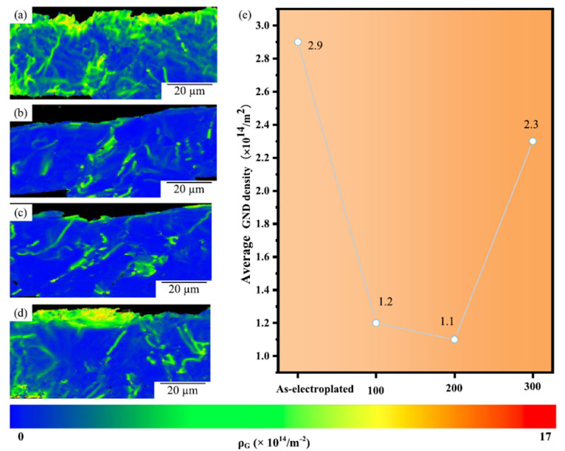
Figure 5. KAM strain distributions at various annealing temperatures.
(Wang et al., 2024, J. Alloys Compd.)1.3 Recrystallization and Phase Transformation Analysis
EBSD can also assess the degree of recrystallization after annealing by comparing crystal orientation maps before and after treatment.
Yang et al. (2024, Micromachines) used EBSD to study annealing behavior in nanotwinned copper. They found that [110]-oriented nanotwinned Cu experienced significant recrystallization, whereas [111]-oriented and randomly oriented Cu showed only minor changes.
GND (Geometrically Necessary Dislocation) analysis showed a significant decrease in overall dislocation density post-annealing, particularly in [111]-oriented Cu, which had the lowest initial and final GND levels (Figures 6 & 7). This highlights the varying thermal stability of copper with different orientations and offers insight into optimizing thermal performance of TGV copper via engineering methods.
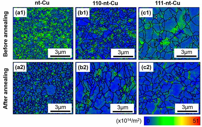
Figure 6. GND maps of nanotwinned Cu before and after annealing.
(Yang et al., 2024, Micromachines)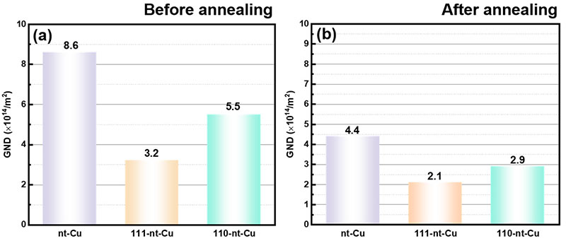
Figure 7. Average GND density changes before and after annealing.
(Yang et al., 2024, Micromachines)1.4 Failure Analysis and Quality Control
EBSD-based failure analysis of TGV structures is still emerging. However, mature applications exist in the TSV (Through-Silicon Via) field, which offers relevant insights. While TSVs go through silicon and TGVs through glass, both face similar issues like stress concentration, copper recrystallization, and thermal mismatch-induced shear stress.
For example, Krause et al. (2011, Proc. IEEE ECTC) developed a failure analysis flow integrating non-destructive defect localization using Lock-in Thermography (LIT) and high-resolution tools (DB-FIB, PFIB, EBSD, TEM) for TSV/μBump structures—providing a practical model for integrated analysis.
Okoro et al. (2021, Microelectron. Reliab.) reported that rapid thermal ramp-up caused thermal stress due to CTE mismatch, forming radial cracks in the glass (Figures 8 & 9). While these cracks didn’t directly affect the copper, they were likely related to grain boundary sliding and copper protrusion.
Zhao et al. (2022, Micromachines) used finite element modeling to show that during cooling, shear stress concentrates at the TGV–Cu interface and around the redistribution layer (RDL) (Figures 10 & 11)—hotspots for grain boundary sliding and local plastic deformation.
If such studies incorporated EBSD to analyze orientation, KAM, or GND near crack origins, they could provide quantitative, geometry-based insights into strain-induced failure mechanisms.
Though dedicated EBSD studies for TGV failure analysis are limited, the technique’s role is expanding—from a passive observation tool to a decision-making core in reliability engineering. Whether for controlling grain size, tracking post-annealing microstructural evolution, or assessing stress fields linked to glass cracking, EBSD offers irreplaceable insights.
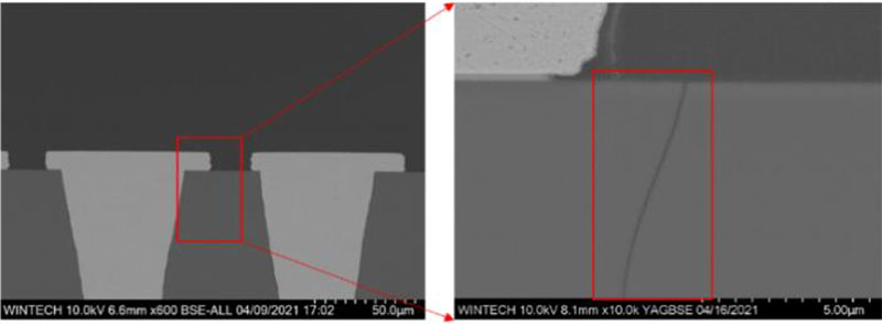
Figure 8. Micro‐cracks at the edges of the TGV and the redistribution layer (RDL) after temperature‐cycling tests.
(Image source: Zhao et al., 2022, Micromachines)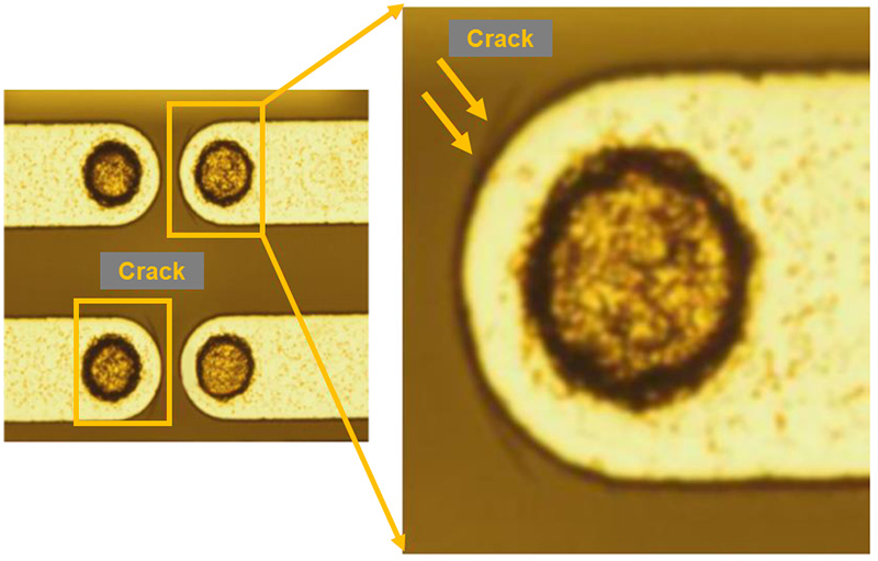
Figure 9. Vertical cracks induced by thermomechanical loading.
(Image source: Zhao et al., 2022, Micromachines)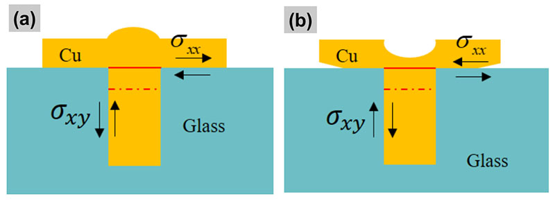
Figure 10. Schematic of shear‐stress distribution inside the TGV structure: (a) during heating, (b) during cooling.
(Image source: Zhao et al., 2022, Micromachines)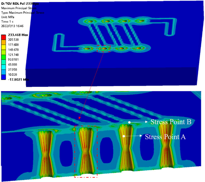
Figure 11. Stress‐concentration zones at the TGV/RDL interface.
(Image source: Zhao et al., 2022, Micromachines)
EBSD is not just a tool for visualizing crystal orientation—it’s a powerful ally for semiconductor engineers aiming to resolve micro-scale failures and enhance packaging reliability. By revealing grain direction, boundary properties, recrystallization, and hidden residual stresses, EBSD plays a vital role in process optimization and material evaluation. Especially in areas near grain boundaries or early crack sites, it allows precise, data-backed insight into micro-strain behavior.
In the future, integrating EBSD with tools like X-ray, SEM, and simulation could establish comprehensive models that span from micro to macro scale—helping process engineers identify risks earlier and address accordingly. In short, EBSD doesn’t just let us “see the direction of crystals”—it helps us “foresee the future of materials.”
Contact Window | Dr. Lin, Wei-jui | Tel:+886-3-5799909#6166 | Email: web_ma@istgroup.com ; marketing_tw@istgroup.com
References:
[1] Y H. Chang et al. “Through glass via (TGV) copper metallization and its microstructure modification”, J. Mater. Res. Technol., 2024.
[2] M. Wang et al. “Effect of heat treatment processes on the Cu electrodeposited through glass vias (TGV) plate”, J. Alloys Compd., 2024.
[3] G. Yang et al. “A study on regulating the residual stress in electroplated Cu by manipulating nanotwin directions”, Micromachines, 2024.
[4] M. Krause et al., “Characterization and Failure Analysis of TSV Interconnects: From Non-destructive Defect Localization to Material Analysis with Nanometer Resolution”, Proc. ECTC, 2011.
[5] C. Okoro et al. “Understanding and eliminating thermo mechanically induced radial cracks in fully metallized TGVsubstrates”, Microelectron. Reliab., 2021.
[6] M. Krause et al., “Characterization and Failure Analysis of TSV Interconnects: From Non-destructive Defect Localization to Material Analysis with Nanometer Resolution,” Proc. ECTC, 2011.