Issued Date:2025/6/12 TEM EELS
Issued By:iST

In TEM compositional analysis, many people still rely entirely on EDS to solve every problem. But when it comes to detecting light elements or analyzing chemical states, the data often appears blurry and difficult to interpret. The issue is not with the instrument’s capability. It is simply that EELS, a powerful and high-resolution technique, has not yet been fully explored.
TEM EELS
Transmission electron microscope (TEM) has been generally accepted to a powerful instrument for analyzing nano-materials due to it atomic resolution power in both image and composition [1]. The manufacture technique of semiconductor devices proceeded into nano nodes in the 21st century, aluminum was replaced by copper in metallization, the structure of transistors was evaluated from planar MOS to 3D Fin. Following the shrinkage in dimension, and change in architecture as well as materials, demands of TEM analyses from R&D in semiconductor devices become more and more. The operation of all current TEMs can be switched between TEM mode and STEM mode with simple alignment due to the progress in TEM operation system.
Requirements of TEM/STEM from semiconductor industry, especially Taiwan’s, have been over those from academia and research community in both quality and quantity. Besides resolution power in images, TEM manufactures have substantially improved the function and the efficiency in composition analysis to meet demands in materials analysis. EDS and EELS are two main attachments in TEM/STEM for composition analysis. The price and the complexity in operation of EELS are much higher than those of EDS, these factors make EDS more popular. However, two characteristics of EELS, high energy resolution and high spatial resolution, have made EELS indispensable in TEM/STEM analysis. The subject of this article is to introduce basic functions and characteristics of EELS.
TEM EELS
TEM EELS
1. Introduction of EELS Spectrum
EELS is the abbreviation of electron energy loss spectroscopy, it is a composition analysis technique used in TEM. This technique collects signals of incident electrons, which are emitted from the electron gun and pass the TEM specimen. These electrons are divided into three categories: un-scattered electrons, elastically scattered electrons, and inelastically scattered electrons. After being collected into the spectrometer, these electrons are deflected by electromagnetic lenses and arranged linearly by their energy, then are magnified properly and sent into an energy detector, finally processed into a spectrum shown in Figure 1, the x-axis is energy loss and the y-axis is intensity (or counts). A whole EELS spectrum includes three regions: the zero-loss peak, low loss region, and core loss region [2].
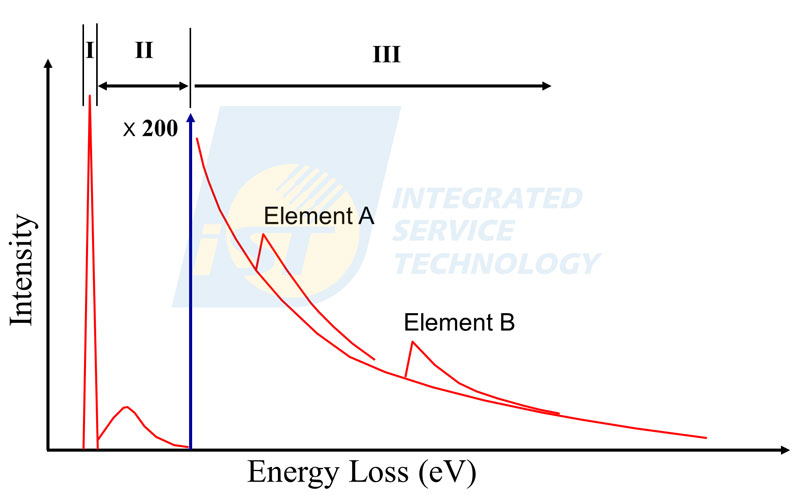
Figure 1: A schematic of a whole EELS spectrum. A whole EELS spectrum is divided into three regions, (I) zero loss peak (-5.0 ~ 5.0 eV),
(II) low loss regions (5.0 ~ 50.0 eV), (III) core loss region (> 50.0 eV).
(Source: iST)The zero-loss peak consists of un-scattered electrons and elastically scattered electrons. The total intensity of the zero-loss peak is more than 98% of the whole EELS spectrum for a thin enough specimen. The shape of the zero-loss peak is close to a sharp Gaussian peak with the peak locating at 0 eV. The low loss region, consisting of inelastically scattered electrons by outer shell of atoms in the specimen, extends from 5.0 eV to 50.0 eV. The shape of low loss peak is a broad Gaussian peak with a little distortion, and its peak position changes with materials analyzed, roughly around 15.0 to 30.0 eV. Regions behind 50 eV is the core loss region which consists of inelastically scattered electrons by inner shell of atoms in the specimen. The signal in the core loss region drop gradually is the background intensity. At some specified energies, some signals increasing quickly and decreasing slowly are superimposed on the smoothly decreasing background. These are signals of inelastically scattered electrons by inner shells of elements in the specimen analyzed. Shapes of elemental signals above the background are similar to saw-teeth and called edges instead of peaks.
Furthermore, these edges are then named characteristic edges because their threshold energies standing for bonding energies of elements in the specimen and fine structure reflecting crystallographic or energy-band structure of elements in the specimen. Elements can be identified by judging the threshold energy firstly, such as 284 eV for carbon and 532 eV for oxygen.
The difference in intensity among these three regions is more than three orders. For an idea TEM specimen for EELS analysis, its thickness should fall in the range of single scattering of incident electrons when they pass through the specimen. When an EELS spectrum was collected from a thin specimen by a TEM operated at 200 KV, if the intensity of zero loss peak is Io, the intensity of low loss peak will be 0.01 Io, and the maximum intensity of Si L edge is about 1 x 10⁻³ Io, the maximum intensity of C K edge is about 0.1 x 10⁻³ Io, the maximum intensity of O K edge is about 0.04 x 10⁻³ Io, etc. The intensity of signals drops quickly with increasing energy loss, as shown in Figure 2.
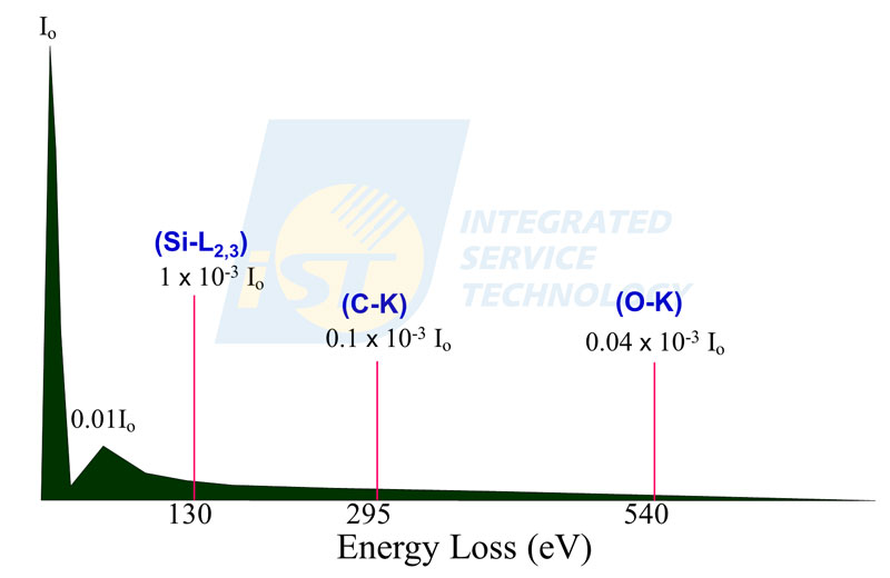
Figure 2: A schematic diagram of a whole EELS spectrum. The intensity of signals in the EELS spectrum drops quickly with the energy loss.
(Source: iST)Since the large variation in intensity and high energy resolution, an actual EESL spectrum is usually displayed in partial region only rather than in full scale. Conventionally, the spectrum showing chemical bonding will be displayed in the range of 150 ~ 200eV, and the spectrum showing elements will be displayed in the range of 400 ~ 600eV, as shown in Figure 3.
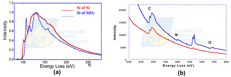
Figure 3: Typical EELS spectra.(a) EELS spectra for Si-L edges of silicon and silicon dioxide, display range ~200 eV.(b) EELS spectra for composition analysis, display range 400 eV.
(Source: iST)When the energy range is over 600 eV, the intensity of characteristic edge of high energy loss may be too small to be observed. Local magnification is then required when this kind of situation happens. When we look back data in the Figure 2, we find that the intensity of Si-L edge is usually 25 times of that of O-K edge. The EELS spectrum of SiO2 will be the way shown in Figure 4(a), the O-K edge is hard to be seen. We have to magnify the y-axis to make O-K edge visible easily as shown in Figure 4(b). However, this make the low energy loss region saturated, and the Si-L edge disappears.
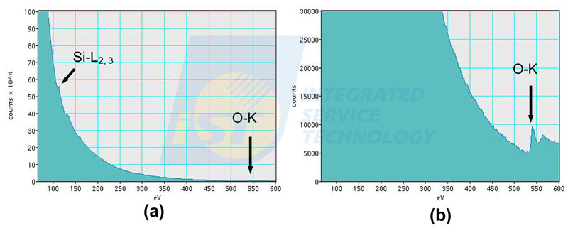
Figure 4. An EELS spectrum of SiO2, display range ~560 eV.
(a)S-L edge is visible, but the intensity of O-K edge is too low to be visible.
(b) O-K edge is visible by magnifying the y-axis, but low energy loss region is saturated.
(Source: iST)Characteristic edges of elements in EELS spectra have K, L, M groups, as energy peaks in EDS spectra. Edges formed by incident electrons inelastically scattered by K shell are called K-edges, so are L-edges and M-edges. Edges in EELS spectra can be marked simply by name of element only, such as C, N, and O shown in Figure 3, or marked by name of element and ionization shell, such as Si-L2,3 and O-K shown in Figure 4.
2. EELS Mapping
EELS mapping can be performed either in TEM mode or in STEM mode, while EDS mapping can only be performed in STEM mode. When EELS mapping is performed in TEM, each elemental map needs to process three images of setting-specific energy windows, two pre-edge images (I & II) and a post-edge image (III), as shown in Figure 5.
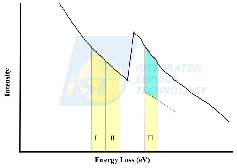
Figure 5: A schematic diagram shows the setting of energy windows for the EELS mapping of three-energy-window method. Both energy window I and energy window II are pre-edge windows and contain background signals only, energy window III is the post-edge window containing signals of element and background.
(Source: iST)Two pre-edge images are images of background signals, and the post-edge image is the image containing signals and background. The part of background in the post-edge image (light yellow part) is calculated by those two pre-edge images. The net signal (light green part) of background subtracted is the elemental signal. An elemental map is obtained by subtracting background in all pixels in image III. One set of images of pre-edge and post-edge, and an elemental map are shown in Figure 6. Obviously, images of three individual image (Figure 6b, 6c, 6d) are not able to tell nitrogen distribution exactly. Only the processed image can display nitrogen distribution correctly, as shown in Figure 6(e).
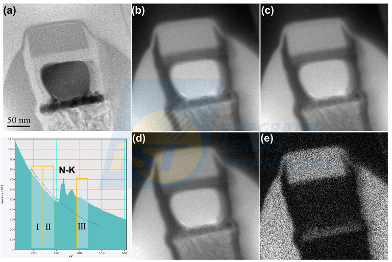
Figure 6. EELS analysis of a semiconductor device. (a) BF image, (b) N pre-edge image I, (c) N pre-edge image II, (d) N post-edge image, (e) N elemental map. A corresponding EELS spectrum containing N K edge is inserted at lower left corner, three energy windows included.
(Source: iST)Most of current EELS mapping are performed in STEM mode. STEM/EELS mapping is performed by spectrum image technique as STM/EDS mapping does. That means a corresponding EELS spectrum is recorded in each pixel in the STEM image. All elemental maps can then be processed off-line by setting three adequate energy windows.
3. Simple Comparison between EDS and EELS
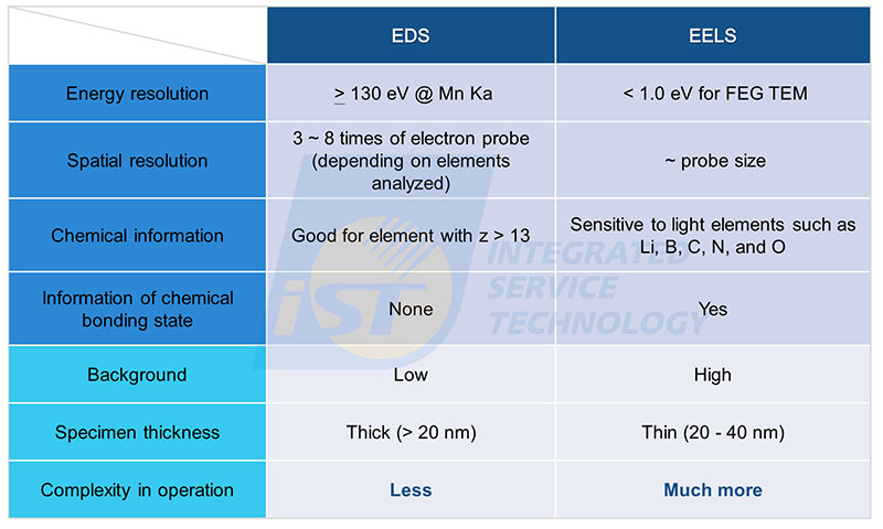
A simple comparison of advantages and disadvantages between TEM/EDS and TEM/EELS are listed in table 1. The greatest strengths of EELS is high energy resolution, this advantage makes it possible to characterize chemical bonding state of elements, while the greatest weakness of EELS is its complexity in both operation and data process. For accurate EELS quantitative analysis, the TEM specimen thickness must be thinner than the average mean free path of inelastic scattering (L) to avoid plural scattering issues for incident electrons. The value of L increases with the acceleration voltage of TEM and decreases with the atomic number of elements in the specimen.
Table I. A simple comparison between TEM/EDS and TEM/EELS.
(Source: iST)
Besides EDS, EELS is another nano composition analysis technique using energy to characterize elements. The greatest strengths of EELS is high energy resolution, better than 1.0 eV when FEG TEM is used, so chemical bonding states of elements can be identified. Detection efficiency of EELS for light elements, such as Li, B, C, N, and O, is much better than that of EDS, but reverse for elements of large atomic number.
References:
[1] D. B. Williams and C. B. Carter, in Transmission Electron Microscopy, (2009).
[2] R. F. Egerton, “Electron Energy-Loss Spectroscopy in the Electron Microscope, 2nd edition (1996).