Issued Date: 2019/3/5
Issued By: iST
Most samples subject to tests are solid;
How do we test liquid materials, or suspicious defects found in liquid substances of processing?
In the process of making semiconductors, including wafer fabrication, photolithography etching and thin film, or other electronic products including solar and LED chips, liquid/volatile materials such as silver paste, grinding and polishing fluids, and inks may be employed. All of them may lead to flaws in finished goods.
A scanning electron microscope (SEM) may be used to inspect the surface of most solid samples in a vacuum environment. This is not the case with liquid/volatile materials as they may hamper the SEM vacuum and lead to chamber contamination. That is, SEM inspection may be a tall order in a case like this.
An alternative adopted in most cases is to solidify the liquid/volatile samples by baking them and subject them to SEM inspection. However, this deforms their shape and texture, e.g. the distribution and dispersion of particles in liquid material gets lost and its actual liquid material pattern cannot be observed.
How to deal with this dilemma? This is the focus of today’s iST Tech Classroom:
Employ a liquid material specific SEM platform
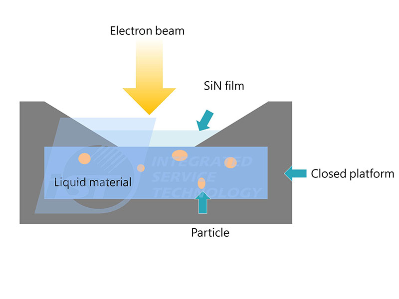
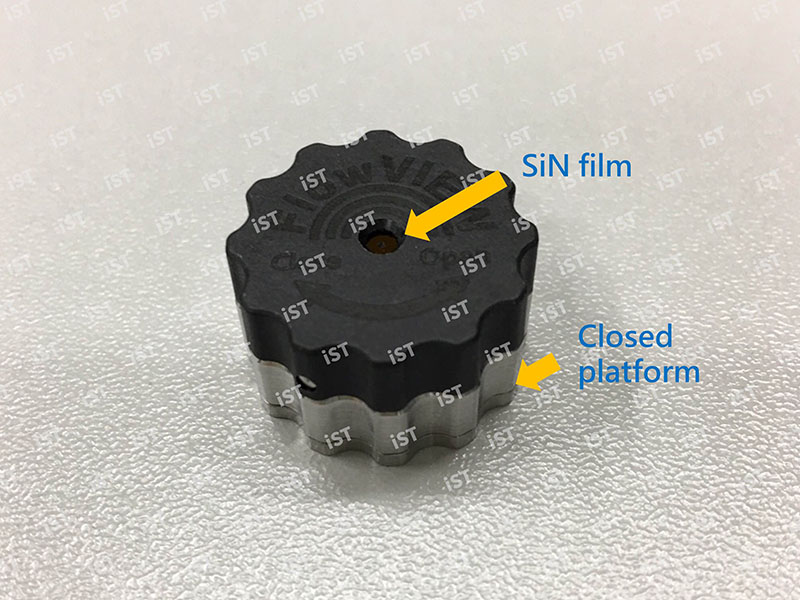
Figure: Liquid sample-specific SEM platform illustration
SEM liquid platform is a closed structure which can enclose liquid/volatile materials with the SiN film of several tens of nanometers thick on the surface of a SEM platform on top. SEM can excite the secondary or the backscattered electrons on the surface of the liquid sample for successful imaging without impact on the SEM vacuum or vacuum system contamination.
Component analysis then can be executed together with energy dispersive spectroscopy (EDS). In addition, SEM images can be analyzed by special software to obtain size distribution, dispersion, shape distribution and other data (see figure below) for material R&D or process improvements and monitoring.
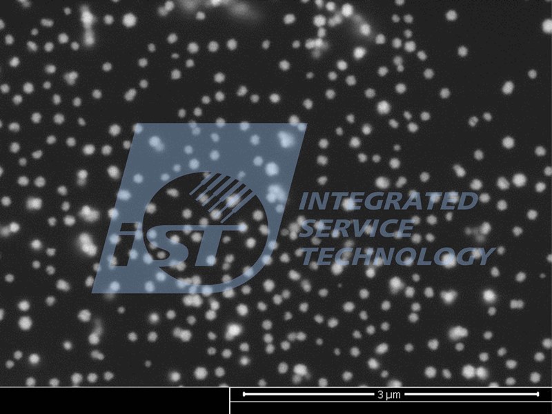
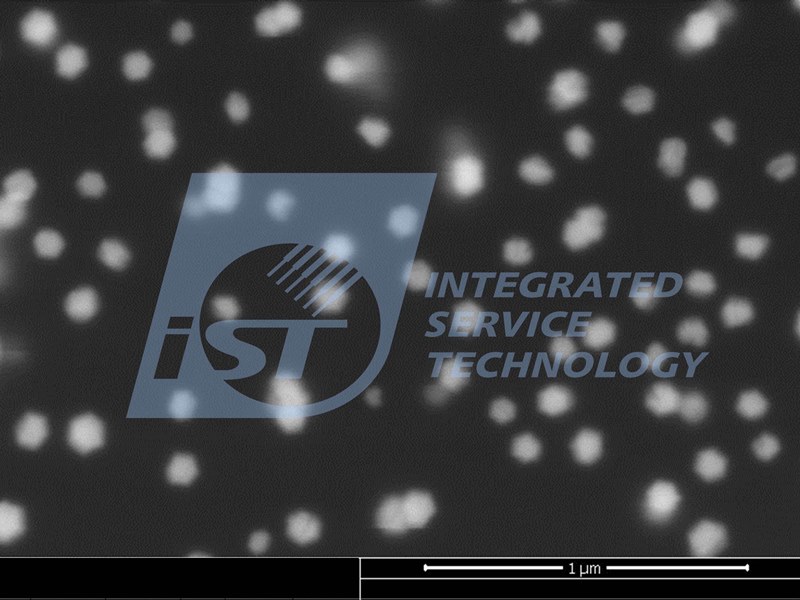
Figure: SEM image of liquid grinding material which show clear distribution and dimension of SiO2 particles
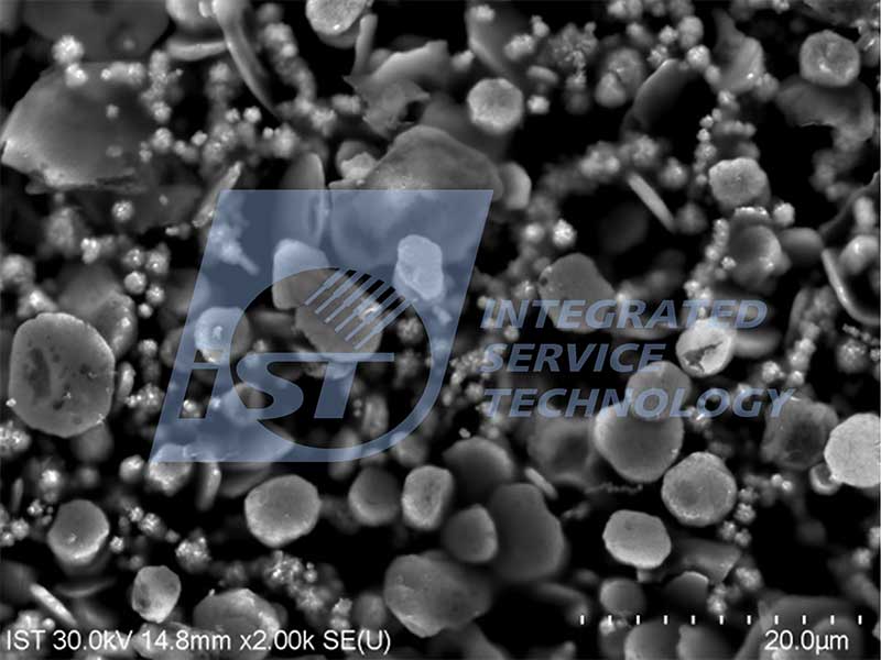
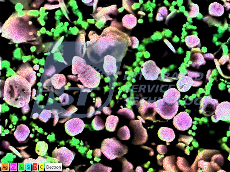
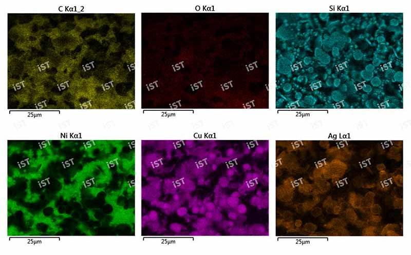
Figure: The element distribution status of liquid material and silver paste can be confirmed using EDS mapping
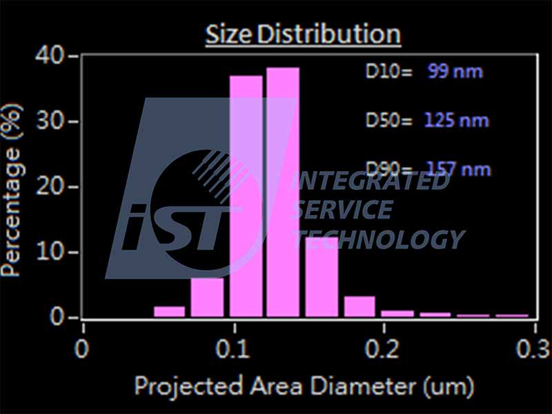
Figure:
Particle size distribution by software analysis
(illustration of particle size proportion)
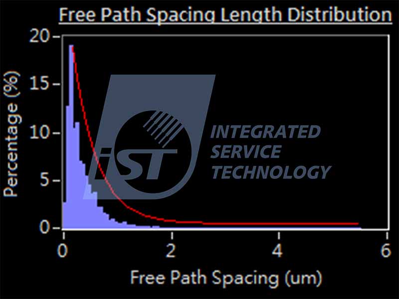
Figure:
Particle dispersion by software analysis
(illustration of particle pitch proportion; the more centralized the better)
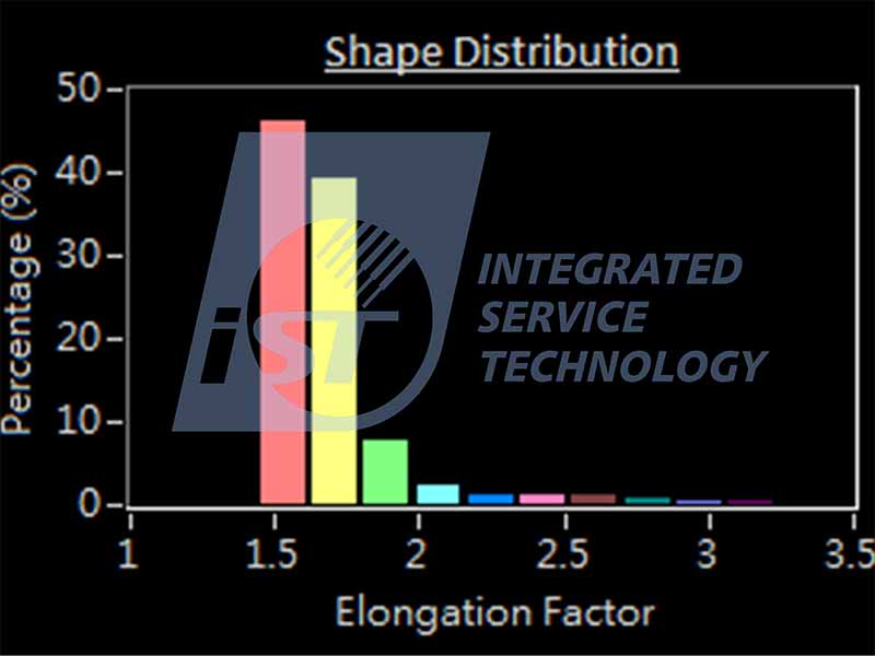
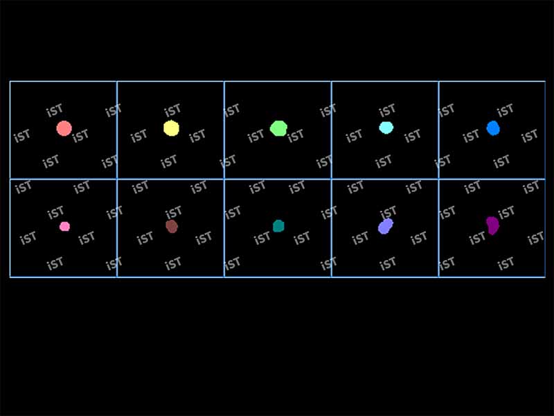
Figure: Particle shape distribution by software analysis
(illustration of shape distribution; the more elongation factor approaches 1, the more the particle shape is close to circularity)
* Thanks to FlowVIEW Tek for its assistance with liquid inspection techniques. More accurate measurement and analysis technology will be provided to enable online monitoring of fluid in production lines.
*【Important Note】The liquid sample inspected in this way must have particles in it, such as silver paste, grinding and polishing fluids, inks, etc.. Liquid without particles such as photoresist fluid, it is not possible to inspect with this method.
This article is aimed to share our experiences with honorable clients like you. In case you want to know more details, please call Mr. Edward Chen at +886-3-579-9909 Ext. 6641 or email: web_pfa@istgroup.com