Issued Date:2025/11/27 SIPI-simulation
Issued By:iST
Your high-speed product runs fast — but does it run stably? In the GHz generation, every trace on your PCB can become a potential failure point. A signal delay of 10-ps or a 1 Ω impedance mismatch can easily derail your product before mass production. With SIPI simulation, hidden electrical risks can be identified early in the design phase — ensuring your product not only works but is ready for volume production.
SIPI-simulation
SIPI-simulation
SIPI-simulation
Is your high-speed product backed by SIPI simulation? For low-speed systems, simulation is often a nice-to-have. But in the high-speed domain, even minor signal distortion or noise can silently impact your system’s performance. Signal Integrity (SI) and Power Integrity (PI) simulation enable designers to predict and correct issues in advance — from eye diagrams and jitter to PDN impedance — transforming late-stage firefighting into early-stage prevention.
Today, achieving functional correctness is no longer enough. As interfaces such as PCIe Gen5/6, DDR5, and USB4 push data rates into the multi-GHz range, even small electrical anomalies can cause data errors, unstable links, and may ultimately prevent the product from reaching the market.
The best defense? Incorporating SIPI simulations during design to uncover risks before fabrication — ensuring higher yield, reliability, and system robustness.
This iST Tech Classroom article walks you through ten essential reasons why SIPI simulation is indispensable for high-speed design, along with a practical step-by-step integration guide. (Read more: iST Launches AI High-Speed Signal Transmission Solution to Help You Lead the Market)
I. Understanding SIPI Fundamentals
SI simulation is a predictive analysis technique for high-speed PCB design. By building accurate models before fabrication, engineers can predict potential anomalies during signal transmission and mitigate electrical risks early. It helps evaluate jitter, attenuation, and crosstalk effects to ensure signal decodability and compliance under GHz-level conditions.
PI simulation focuses on the Power Distribution Network (PDN) — analyzing supply noise, IR drop, and decoupling efficiency to maintain stable voltage delivery. It predicts power noise behavior and transient response under dynamic loading, reducing the risk of power-induced timing errors.
In short, only by combining SI and PI analysis can engineers achieve full system stability and performance assurance.
2. Why SIPI Simulation Matters — 10 Key Questions
In the following Q&A format, we will guide you to understand how SIPI simulation fundamentally boosts design success rates and mitigates risks before failures even occur.
Q1. Why do signal reflections easily occur in high-speed circuits?
Reflection happens when impedance discontinuity occurs at traces, vias, or connectors, causing waveform distortion. In high-speed designs, even minor discontinuities can cause significant waveform distortion, collapsing the eye diagram or leading to receiver misinterpretation.
Q2. Why do adjacent traces interfere with each other?
When traces are placed too close, the electromagnetic fields surrounding them couple together, creating crosstalk. This type of “invisible interference” may cause bit errors or increase BER.
Simulation tools allow us to visualize these hidden coupling effects and recommend optimal spacing, routing, and shielding strategies to maintain signal integrity.Q3. How do we compensate for long-distance signal loss?
Signals attenuate due to conductor and dielectric loss. SIPI simulation evaluates trace geometry, material choices, and equalization techniques (EQ, CTLE, DFE) to maintain eye opening and integrity.
Q4: Can simulation really predict the eye diagram? Can it tell me whether my design will pass?
Absolutely. The eye diagram is the most intuitive indicator of signal quality. With simulation, we can predict eye-opening height and width, check compliance with standards such as USB4 or PCIe Gen5, and verify performance before fabrication—significantly shortening debug cycles.
Q5: How can I ensure timing accuracy and avoid data delay issues?
In high-speed designs, transmission delay and jitter directly impact setup/hold margins, leading to data misalignment. Simulation can precisely predict delay, skew, jitter, and other timing-related parameters for each channel, helping designers guarantee that every bit arrives on time even before layout is finalized.
Q6: How can I ensure the stability of differential signals?
Differential-pair performance depends on symmetry, coupling, and skew. Any imbalance weakens noise immunity and affects stability. SI simulation quantifies skew and common-mode noise, ensuring differential pairs remain robust under high-speed and extreme operating conditions.
Q7: Can SIPI simulation help pass protocol compliance testing?
Yes. Modern high-speed standards (PCIe, USB, DDR, etc.) include strict SI requirements—eye masks, Tx/Rx equalization, return loss, and more. Simulation allows us to predict compliance performance before lab testing, reducing the risk of repeated rework and verification cycles.
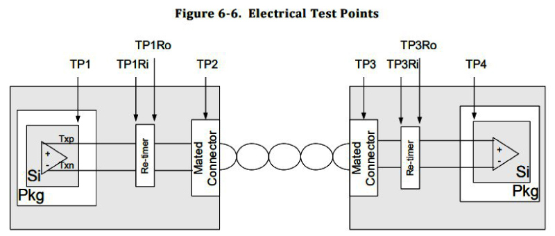
Figure 1: USB test environment and probe points defined in the Universal Serial Bus 3.2 Specification.
(Source: Universal Serial Bus 3.2 Specification)
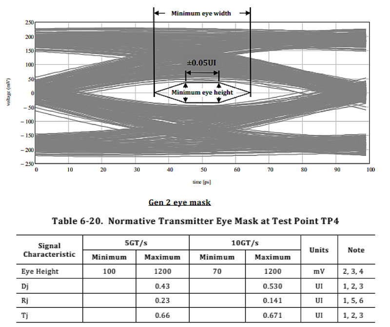
Figure 2: Defined eye-mask compliance region at test point TP4
(Source: Universal Serial Bus 3.2 Specification)Q8: Can simulation help reduce development cost?
A: Definitely. If signal problems are discovered only after PCB fabrication or during lab testing, rework costs can increase by several times—or even tenfold. SIPI simulation identifies risks early in the design phase, preventing re-spins, shortening schedules, and lowering overall development cost.
Q9: What is PDN impedance and why does it impact power delivery?
A: When the Power Distribution Network (PDN) impedance is too high, voltage ripple and IR drop increase, causing instability in high-speed interfaces such as SerDes or DDR5. PI simulation evaluates the PDN impedance profile, optimizes decoupling strategies and stack-up design, and ensures power noise is effectively suppressed.
Q10: How do we predict power transients and IR drop?
A: As switching frequency and current demand rise, transient current spikes become more severe and may cause voltage droop. PI simulation predicts IR drop and transient response under different loading conditions, enabling early correction of PDN design to avoid timing errors and system instability due to insufficient power delivery.
3. Eight Key SIPI Observation Metrics
(1) Eye Diagram
An eye diagram overlays consecutive digital waveform to visually evaluate the stability and reliability of a high-speed signal. Its shape is affected by the combined impact of jitter, loss, crosstalk, and reflections.
In SIPI simulation, engineers can predict eye height and eye width before the PCB is fabricated and verify whether the eye-opening meets protocol-defined eye mask requirements such as PCIe Gen5/6, USB4, or DDR5.
The size of the eye opening is the primary indicator of whether the signal can be correctly decoded and whether it will pass compliance testing.
Figure 3: Eye Diagram Analysis
(Source: iST)(2) Jitter
Jitter refers to the time-domain deviation or fluctuation of a signal’s edge. It includes both Random Jitter (RJ) and Deterministic Jitter (DJ). In high-speed transmission, excessive jitter directly compresses the timing margin and significantly increases bit error probability.
Through simulation, we can identify the root causes of jitter—such as power noise, reflections, or inconsistent trace length—and correct them early, providing greater timing robustness.
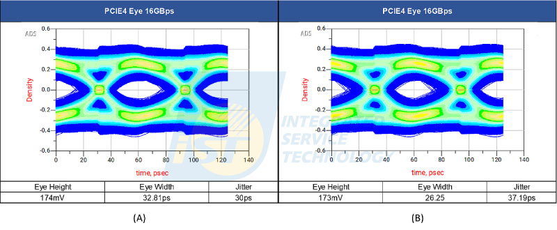
Figure 4: Evaluation of eye diagram impact under different jitter conditions. Left (A): TX DJ = 0.01 UI, RJ = 0 UI; Right (B): TX DJ = 0.05 UI, RJ = 0.02 UI. The eye diagrams at the RX side after channel transmission illustrate how varying simulation parameters help assess jitter and channel effects.
(Source: iST)(3) Skew
Skew occurs when multiple signals experience different propagation delays, creating timing misalignment. It is especially critical in differential pairs and multi-bit parallel buses.
Excessive skew disrupts data synchronization and degrades eye diagram alignment.
Simulation quantifies differences in trace length, symmetry, and propagation delay, enabling optimized routing compensation and symmetric via design to ensure signal synchronization.(4) Impedance Matching
Impedance control is fundamental to stable high-speed transmission. Any impedance discontinuity in traces, vias, or connectors can cause reflections.
Simulation tools use 2D/3D structural modeling to help engineers optimize trace width, layer stack-up, and material selection to maintain impedance uniformity.
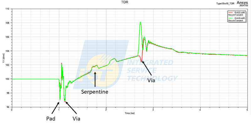
Figure 5: TDR trace results showing delay-based identification of impedance discontinuity locations, enabling structural optimization to reduce reflections.
(Source: iST)(5) S-Parameters
S-parameters are essential frequency-domain analysis tools used to characterize signal behavior across frequencies. Key metrics include S11 (return loss) and S21 (insertion loss), which assess reflection and transmission loss along the channel. In SIPI simulation, scattering matrix models predict channel performance across frequency and verify compliance with IL/RL masks.
S11 (Return Loss): Indicates the proportion of energy reflected back to the transmitter due to impedance mismatches. Reflections occur at structural transitions such as vias, connectors, or trace geometry changes. Simulation predicts these reflections and guides impedance tuning to minimize waveform distortion and interference.
S21 (Insertion Loss): Represents signal attenuation caused by conductor and dielectric loss. Higher IL indicates faster signal degradation and eye collapse. Simulation evaluates IL across frequency under different materials, lengths, and routing structures, enabling selection of low-loss materials or appropriate compensation—such as re-timers or stack-up adjustments—to maintain signal integrity.
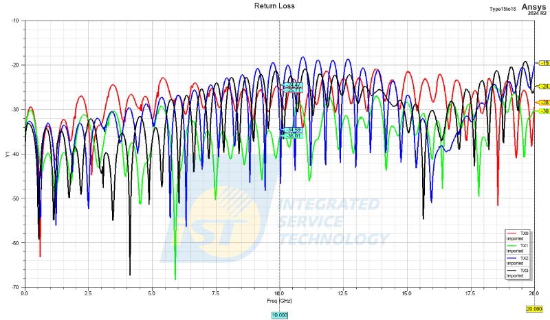
Figure 6: The S11 result indicates whether modifications to the trace design are necessary. Industry specifications typically define a maximum allowable dB level for return loss.
(Source: iST)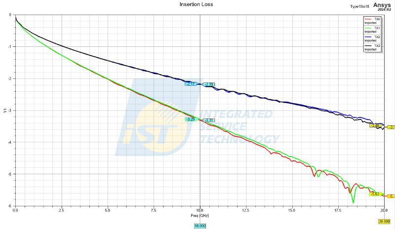
Figure 7: The S21 results indicate whether the design exceeds the specification limits, helping determine if adjustments to trace routing, length, stack-up, or material selection are required.
(Source: iST)(6) Crosstalk
Crosstalk occurs when adjacent traces are routed too closely, causing their electric and magnetic fields to couple and generate near-end (NEXT) and far-end (FEXT) interference.
Simulation evaluates spacing, layer structure, and coupling effects, and provides routing, guard-trace, and ground-shielding recommendations to prevent system errors and increased BER.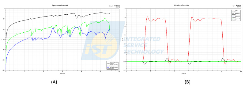
Figure 8: Crosstalk observed on the victim line in both frequency and time domains. Left (A): frequency-domain results; Right (B): time-domain results. The black, green, and blue curves represent the impact from different aggressor sources on the victim signal.
(Source: iST)(7) BER (Bit Error Rate)
BER represents the number of bit errors that occur over a given number of transmitted bits—an essential indicator of system reliability. SI simulation predicts BER bathtub curves under varying jitter and loss conditions and helps determine whether FEC (Forward Error Correction) or EQ (Equalization) adjustments are required to ensure signal decodability under worst-case scenarios.
(8) Equalization
To compensate for waveform distortion caused by long channels and high-loss media, systems rely on transmitter pre-emphasis and receiver equalization (CTLE, DFE). These techniques restore the waveform quality. SIPI simulation evaluates different EQ configurations and quantifies their improvements to the eye opening, helping engineers choose the optimal balance of performance and power—particularly valuable for high-speed backplanes and connector-rich designs.
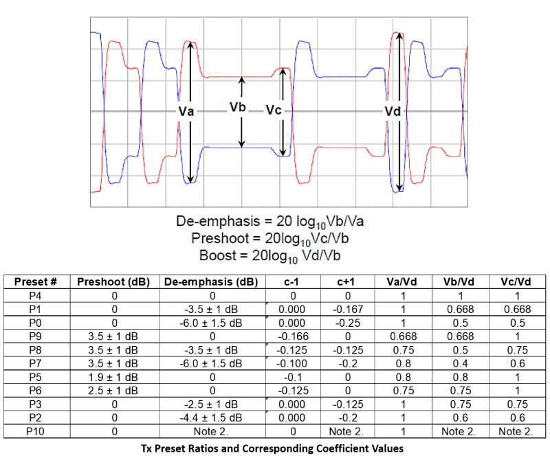
Figure 9: PCIe transmitter (TX) preset equalization settings. High-frequency components are pre-emphasized at the IC transmitter to compensate for channel high-frequency loss in advance, resulting in a more stable waveform at the receiver.
(Source: PCI Express Base Specification Rev. 4.0 Version 1.0)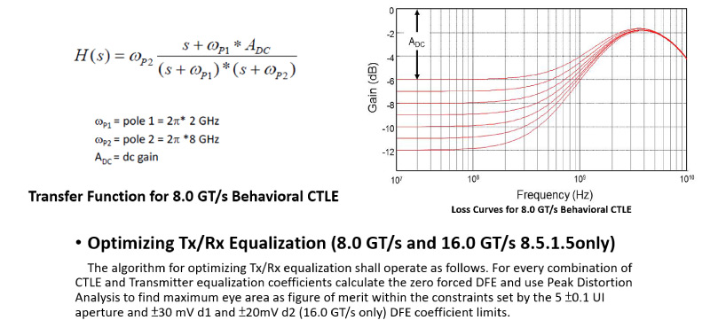
Figure 10: PCIe receiver equalization: CTLE boosts high-frequency content while attenuating low frequency, and DFE further suppresses noise, improving crosstalk and ISI performance.
(Source: PCI Express Base Specification Rev. 4.0 Version 1.0)4. Recommended SIPI Implementation Flow: From Modeling to Validation
To maximize the benefits of SIPI simulation, iST recommends the following workflow:
- Build a Model Library
Collect IBIS/SPICE component models, interconnect S-parameters, and PDN data to establish a complete signal–power simulation database. - Pre-Simulation Analysis (Pre-sim)
Evaluate transmission loss, impedance discontinuities, routing topology, and PDN impedance distribution early in the design process to ensure stable power delivery. - Post-Simulation Validation (Post-sim)
Import the actual PCB layout and perform full SI/PI simulation—validating eye diagrams, jitter, timing margin, and PDN noise performance. - Design Optimization
Adjust stack-up, routing, terminations, and decoupling-capacitor placement/quantity based on simulation feedback to balance performance and cost. - Physical Test Correlation
Perform laboratory measurements and correlate the results with simulation data. Iteratively refine model accuracy to ensure reliable, high-fidelity SIPI simulation.
- Build a Model Library
In today’s semiconductor and electronic design landscape, high-speed signaling has shifted from a “value-added enhancement” to a fundamental requirement. Implementing SIPI simulation allows engineers to identify risks early, minimize design iterations, shorten development cycles, and reduce costly lab rework—ultimately lowering engineering and schedule risk.
For further consultation or technical details, please contact us:
+886-3-579-9909 ext. 8890 (Ms. Lin) Email: HWBU_Sales@istgroup.com | marketing_tw@istgroup.com