Issued Date:2025/11/11IC substrate
Issued By:iST
In the early stages of R&D, engineers frequently face the same challenges: the quantity of IC Engineering Substrate samples is too small, making major manufacturers unwilling to accept the order. Even more troublesome, once the boards are finally secured, engineers still need to find a packaging house for die mount, which is time-consuming and labor-intensive, severely dragging down the verification timeline.
IC substrate
IC substrate
When chip design enters the EVT/DVT (Engineering Verification Test / Design Verification Test) phases, engineers urgently need substrates for functional testing and electrical verification. However, the current market landscape presents several distinct problems:
- Major Manufacturers Focus on Mass Production, Neglecting Small Volume Samples
Mainstream IC substrate suppliers prioritize large customers and high-volume mass production. They offer limited support for the small-batch needs (5–100 pieces) typical of the R&D stage, making it difficult to obtain engineering samples. - Excessive Lead Times Stall R&D Schedule
Traditional substrate manufacturers often have production schedules that span 2–3 months. This directly contradicts the requirement for fast, precise, and decisive action characteristic of engineering verification. For IC design companies, R&D speed is directly tied to securing first-mover advantage in the market. - Advanced Packaging Technologies Increase Verification Difficulty
Under new architectures like CoWoS, Chiplet, and multi-die integration, multiple heterogeneous chips can be combined in a single package for final testing. However, during the development and verification period, performing verification on a single chip within that complex system becomes extremely difficult. This is mainly because a separate, dedicated substrate for that specific chip must be designed. Traditional methods like COB (Chip-on-Board) wire bonding or simple single-engineering boards are insufficient to support these high-density, high-bandwidth verification needs. - Increasing Design Complexity Strains PCB Technology
As process nodes continuously shrink and chip I/O counts surge, the requirements for Pitch, Line Width/Spacing become increasingly stringent. General PCB technology struggles to break through these limitations. This means that even when engineers have a solid design, they cannot find a manufacturing partner capable of rapid execution.
iST’s “One-stop IC Engineering Substrate” Service Solves Your Pain Points
iST has heard the extensive needs of its customers and launched the “One-stop IC Engineering Substrate Service,” specifically built for R&D verification.
You only need to provide the wafers/dies under test. Subsequently, the entire process—from Substrate Layout Design, Signal/Power Integrity Simulation (SI/PI), Specification Confirmation (Spec), to Die Mount—can be completed in a single iST Turnkey solution, saving you the trouble of coordinating with multiple parties.

Figure 1: iST’s “One-Stop IC Engineering Substrate” Service
(Source: iST)
- Rapid Turnaround Time: Through optimized internal processes, iST delivers lead times up to 2× faster than traditional large-scale suppliers. For engineering substrates up to 12 layers, delivery can be completed within three weeks, enabling faster development cycles and improved control over R&D schedules.
- Flexible Small-Volume Prototyping: We support small-batch engineering orders from 5 to 100 pieces, eliminating concerns over Minimum Order Quantity (MOQ).
- Complete Design-to-Verification Linkage: We assist customers in a seamless, end-to-end process: from Substrate Layout and SI/PI Simulation, through Die Mount to produce a verifiable IC package, and the subsequent design/manufacturing/assembly of the necessary Test Interfaces (Socket / Evaluation board / Load board / Burn-in board) required during the verification stage. This significantly shortens the customer’s verification cycle.
- Professional Laboratory Support: Directly link with iST’s services for Reliability Testing, Thermal Cycling, and Electrical Verification, achieving an all-in-one solution.
- Heterogeneous Integration Experience: We support high-frequency, high-speed, multi-layer packaging requirements, covering emerging applications such as AI/HPC, 5G/6G, and Automotive Chips.
- Cross-Platform Compatibility: Accelerate implementation and mass production planning by ensuring compatibility with existing Probe Card, Load Board, and Socket test platforms.
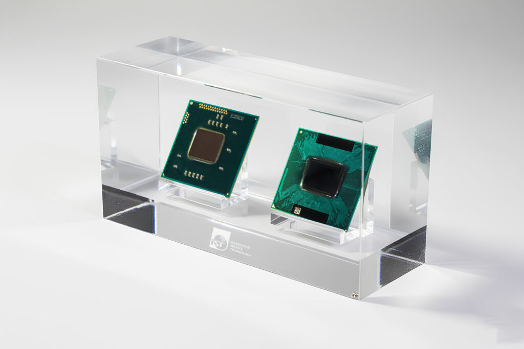
Figure 2: iST Die Mount Substrate
(Source: iST)
Interested in receiving the “iST’s One-stop IC Engineering Substrate”
specification sheet? Email to marketing_tw@istgroup.com to get in touch, or call our hotline: Ms. Aaliyah Lin | Tel: +886-3-579-9909 ext. 8890 | Email: HWBU_Sales@istgroup.com.
Ensure your IC design receives the most reliable engineering verification support from day one.