Issued Date:2026/04/14 SiPh Failure
Issued By:iST
In the architecture of Silicon Photonics, once the Heterogeneous Integration or assembly process is finalized, the module is virtually non-reworkable. How can you ensure that an expensive ASIC isn’t scrapped due to a marginal failure in a single PIC component? This article deconstructs the representative failure modes within the five core functional blocks of a PIC, providing the technical roadmap to overcome the challenges of high-precision alignment in mass production.
SiPh Failure
SiPh Failure
NVIDIA’S Jensen Huang projects that AI infrastructure will reach a trillion-dollar scale by 2027; however, transmission bottlenecks currently limit GPU utilization to under 20%. To overcome these constraints, NVIDIA and TSMC are aggressively advancing Co-Packaged Optics (CPO). By leveraging COUPE technology to achieve 3D Heterogeneous Integration of electronic and photonic components, 2026 is poised to be the inaugural year of mass production.
Nevertheless, the transition from electrical to optical interconnects presents an entirely new landscape. Engineers are no longer merely contending with electrical leakage, but also with complex challenges such as optical loss, coupling misalignment, and signal attenuation. As designs evolve into physical products, the ultimate challenge lies in implementing rigorous verification to ensure the long-term reliability and mission profile of this high-value technology.
Building upon our previous series—from analyzing the core components and performance benchmarks of Silicon Photonics (Read More: “Optical” Breakthrough: Silicon Photonics Chips Ready to Launch), to provide strategic solutions for development hurdles (Read More: Why Silicon Photonics Development So Hard? Verification is the Key), and identifying the critical path to mass production (Read More: Silicon Photonics CPO Nears Mass-Production Breakthrough?)—we continue our deep dive into the SiPh ecosystem.
Continuing our journey, we invite IC engineers to shift their perspective from acting as “neurologists” diagnosing electrical circuitry to becoming “ophthalmologists” treating the complex optics of Silicon Photonics. This article provides a comprehensive deconstruction of the operational principles, prevalent failure modes, and cutting-edge Failure Analysis (FA) techniques for the five core components of a Photonic Integrated Circuit (PIC). Our goal is to empower the industry with the technical clarity needed to master the final hurdles of Silicon Photonics mass production.
I. Three Core Architectures of CPO: From Discrete Plug-ins to Heterogeneous Integration
The fundamental concept of CPO is the integration of previously discrete optical transceivers and high-end switch or computing chips onto a single package substrate. This significantly shortens electrical signal transmission distances, thereby reducing power consumption and latency.
The CPO architecture consists of three core functional units: the ASIC, which acts as the system’s computing brain; the EIC, serving as the electrical signal bridge; and the PIC, which executes electro-optical conversion and transmission. During operation, electrical signals processed by the ASIC are driven and amplified by the EIC, then handed over to the PIC to be converted into optical signals for high-speed transmission. While this tight integration delivers a quantum leap in performance, it also introduces significant quality challenges inherent to electro-optical convergence
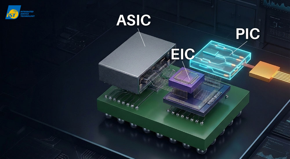
Figure 1: The Three Core Architectures of CPO—ASIC, EIC, and PIC.
(Source: iST — AI-Assisted Generation)II.Stop Saying the Customer Didn't Ask! The AEC Standards Are Crystal Clear
While the industry is well-versed in the failure modes of ASICs and EICs, the Photonic Integrated Circuit (PIC) remains the most unfamiliar territory in CPO verification. Each of the five core components within a PIC operates under unique physical mechanisms, leading to entirely distinct failure pathways. Precisely locating and isolating these microscopic anomalies relies heavily on cutting-edge Failure Analysis (FA) techniques to achieve final risk convergence before mass production.

Figure 2: Schematic of the Five Core Components of a PIC Chip. Each component possesses unique physical mechanisms and failure modes.
(Source: iST — AI-Assisted Generation)1.Grating Couplers (GC):
(1)Operational Principle
Grating Couplers utilize periodic trench structures to enable external optical fibers to couple into chip waveguides at specific angles. This process requires precise calculations of coupling angles and dimensions, as these factors directly dictate light-gathering efficiency and polarization selectivity.
(2)Representative Failure Modes
Surface morphology variations driven by alignment deviations, process residues, or environmental particle contamination can lead to performance degradation. Additionally, physical damage caused by mechanical stress often triggers optical leakage or significant wavelength shifts.
(3)Analytical Techniques
The iST Laboratory utilizes Scanning Electron Microscope (SEM), Energy Dispersive X-ray Spectroscopy (EDX), Dual beam FIB, and Transmission Electron Microscopy (TEM) to perform microscopic defect analysis. Furthermore, cross sectional inspections are employed to verify the physical integrity of the laser to grating coupling interface.2.Waveguides (WG):
(1)Operational Principle
Waveguides serve as the primary channels for optical transmission. They utilize the refractive index contrast between the core and cladding materials to achieve total internal reflection, effectively confining the light beam within the channel. Silicon, silicon nitride, and silicon carbide are commonly utilized materials for this purpose.
(2)Representative Failure Modes
Material absorption rates must be rigorously examined, as excessive absorption leads to significant transmission attenuation. Furthermore, sidewall roughness of the waveguide can trigger scattering loss, while thermal stability remains a critical factor due to its direct impact on the refractive index.
(3)Analytical Techniques
The iST Laboratory performs precision cross sectional analysis to observe whether the structural dimensions of the waveguide transmission channels align with the original design. This process also involves inspection for structural variations or defects that could result in optical signal loss.3.Heaters:
(1)Operational Principle
Heaters generate thermal energy via electrical current to locally modify the waveguide temperature, inducing refractive index changes for precise phase tuning. Common materials utilized for these components include Titanium (Ti), Tungsten (W), and Titanium Nitride (TiN).
(2)Representative Failure Modes
Insufficient spacing between conductive lines or poor insulation can easily lead to electrical leakage or even catastrophic structural burnout caused by Electrostatic Discharge (ESD). Furthermore, inadequate thermal isolation may result in thermal crosstalk, interfering with adjacent components.
(3)Analytical Techniques
The iST Laboratory performs cross sectional inspections specifically targeting leakage points. This is complemented by precision IC Delayer to identify the exact location of burnout or leakage sites layer by layer.4.PN Junction Modulator:
(1)Operational Principle
PN Junction Modulators apply a reverse bias to the PN junction to alter the depletion region’s width, thereby modulating the refractive index and the speed of light. Utilizing interference principles, this process converts electrical signals (0s and 1s) into high speed optical signals.
(2)Representative Failure Modes
Common issues include high temperature induced transient failures as thermal drift, permanent ESD breakdown, and modulation inefficiency caused by variations in ion implantation concentration.
(3)Analytical Techniques
The iST Laboratory utilizes Scanning Capacitance Microscopy (SCM) or Atomic Force Microscopy (AFM) to visualize carrier concentrations and doping profiles, ensuring they align with the original design specifications. Furthermore, cross sectional inspections of the PN junction remain an indispensable part of the verification process.5.Ge Photodiodes, PD:
(1)Operational Principle
Photodiodes are responsible for converting optical signals back into electrical signals. In the industry, Germanium (Ge) is commonly integrated into the silicon process to significantly enhance sensing sensitivity for specific optical wavelengths.
(2)Representative Failure Modes
The most critical failure is dark current issue. This typically originates from lattice defects during epitaxial growth or metallic micro-contamination such as residual Gold (Au) or Aluminum (Al), which can create leakage paths. Other failures include component degradation or physical burnout caused by external thermal stress, prolonged improper hardware operation, or sudden high-current surges.
(3)Analytical Techniques
Analyzing Germanium photodiodes is extremely challenging. iST utilizes Electron Beam Induced Current (EBIC) technology for high resolution electrical failure localization. This is further supported by Transmission Electron Microscopy (TEM), Energy Dispersive X-ray Spectroscopy (EDX), and Secondary Ion Mass Spectrometry (SIMS) for in depth lattice defect and metallic contamination analysis, ensuring the root cause of Ge photodiode failure is identified.III. The Ultimate Hurdle in Testing and Mass Production: Blind Alignment and the Mathematical Trap of KGD
When scaling silicon photonics to mass production, engineers encounter challenges fundamentally different from those in traditional IC manufacturing. This is not merely a struggle against physical limits; it is trade-off involving cost and yield.
(1) Optical Coupling’s “Blind Operation “
Aligning light into a waveguide thinner than a human hair requires an alignment tolerance within 0.5µm. In traditional testing, the need for repetitive refocusing and angular adjustments leads to extremely low throughput and exorbitant time costs, directly dragging down the product’s time-to-market (TTM).
(2) The KGD (Known Good Die) Yield Multiplication Trap
Under a heterogeneous integration architecture, the total yield is the product of each individual component’s yield. If a PIC is found to be defective after packaging, the loss is not just a low-cost component, but also the high-end ASIC—valued at thousands of dollars—packaged alongside it. This “small part dragging down a big chip” risk is a fatal blow that can reduce gross margins to zero.
(3) The Limits of Traditional Inference Methods
In the past, Optical Wafer Acceptance Testing (OWAT) relied heavily on reflection measurements, which only provided the “Total Insertion Loss.” Engineers were unable to determine exact optical loss values or identify “microscopic anomalies” before packaging, allowing risks to be carried all the way into the final production line.IV. Verification Standards and Breakthroughs: From ``Inference`` to ``Visualized`` Precision Measurement
To bridge testing blind spots, the industry has established a dual-track defense consisting of Qualitative and Quantitative analysis. Referencing the carrier-grade Telcordia GR-468 standard, verification is executed across five levels, ranging from the wafer (Level 1) to the fully integrated module (Level 5).
This regulatory framework encompasses more than just “Pass/Fail” qualitative physical stress testing; it emphasizes in-situ (real-time) dynamic monitoring. By continuously tracking critical parameters—such as minimum laser current threshold, wavelength drift, photodiode responsivity and extinction ratio—engineers can precisely capture the microscopic anomalies that lead to system failure, achieving full visualization of the verification process.
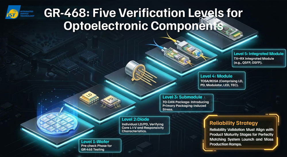
Figure 3: Schematic of GR-468 Standards. The complete lifecycle from wafer to final integrated module can be categorized into five verification levels.
(Source: iST — AI-Assisted Generation)
Silicon Photonics and CPO are the undeniable heart of the next-generation AI era. However, the complex failure analysis pathways and yield traps hidden behind optoelectronic integration represent a formidable challenge for engineers. Overcoming these hurdles requires more than just trial and error; it demands a precise “Qualitative and Quantitative” dual-track analysis to transform unknown risks into controllable data.
If you are currently at a critical stage of Silicon Photonics R&D, we invite you to contact us immediately. Let iST’s expert team serve as your technical backbone to conquer mass production bottlenecks together!
📞 +886-3-5799909 Ext. 1065 (Ms. Chen) 📧 marketing_tw@istgroup.com